Silicon carbide semiconductor device and method for manufacturing the silicon carbide semiconductor device

a semiconductor device and silicon carbide technology, applied in the direction of semiconductor devices, electrical devices, transistors, etc., can solve the problems of narrow process margin, insufficient breakdown voltage, and reduced adhesion between the source electrode and the bonding wire, so as to simplify the manufacturing process and increase the process margin

Inactive Publication Date: 2016-05-12
TOYOTA JIDOSHA KK
View PDF0 Cites 20 Cited by
  • Summary
  • Abstract
  • Description
  • Claims
  • Application Information

AI Technical Summary

Benefits of technology

[0019]Thus, such a simultaneous formation of a trench and a mesa structure can unify the processes for formation of the trench and the mesa, and thus simplify the manufacturing process. In the formation of the trench, the second recess formed in the source region allows the trench to be formed at a position deeper than the mesa structure.
[0020]Accordingly, the height of the protruding trench from the base region toward ...

Problems solved by technology

The excessively deep mesa structure, however, leads to a reduction in thickness of a p-type RESURF layer and a p-type guard ring layer formed on the mesa structure, resulting in insufficient breakdown voltage.
The requirement of such precise depth control results in a narrow process margin.
The excess protrusion of the interlayer insulating film from the substrate, however, causes step differences in the source electrode, resulting in disadvantages, such as a reduction in adhesion between the source electrode and bonding wires, an...

Method used


Image

  • Silicon carbide semiconductor device and method for manufacturing the silicon carbide semiconductor device
  • Silicon carbide semiconductor device and method for manufacturing the silicon carbide semiconductor device
  • Silicon carbide semiconductor device and method for manufacturing the silicon carbide semiconductor device

Examples


first embodiment

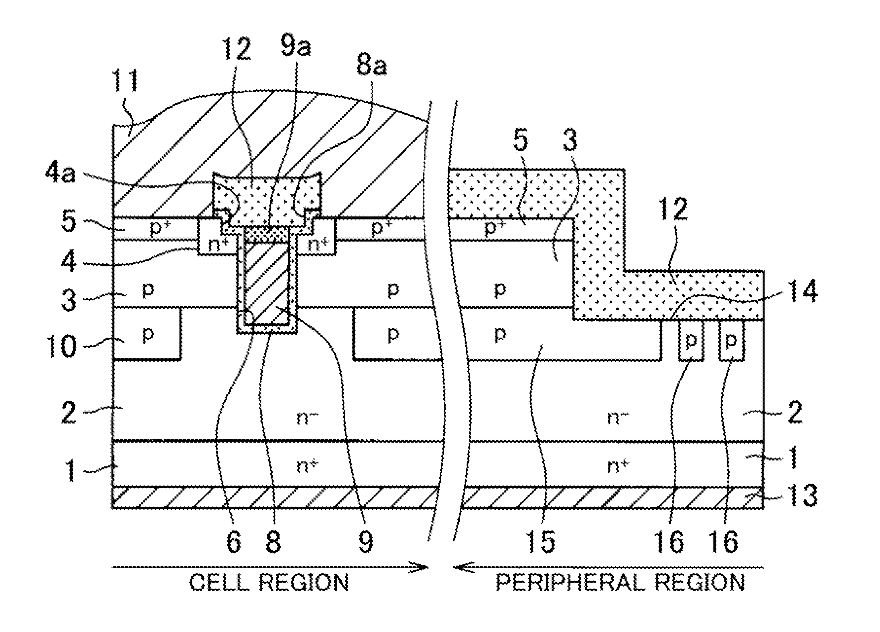
[0042]A first embodiment of the invention will be described. A SiC semiconductor device according to the first embodiment includes a cell region having a MOSFET and a peripheral region having a peripheral high-breakdown-voltage structure surrounding the cell region as shown in FIG. 1.

[0043]The SiC semiconductor device includes an n+-type SiC semiconductor substrate 1 having a principal surface of a Si-plane (i.e., the direction perpendicular to the substrate is the direction of plane [0001]), a concentration of an n-type impurity, such as nitrogen, of, for example, 1.0×10¹⁹ / cm3, and a thickness of about 300 μm. An n−-type SiC drift layer 2 having a concentration of an n-type impurity, such as nitrogen, of, for example, 3.0×10¹⁵ to 10.0×10¹⁵ / cm3 and a thickness of about 5 to 15 μm is formed on the surface of the n+-type substrate 1. Although the impurity concentration of the n−-type drift layer 2 can be constant in the depth direction, the concentration is preferably gradually varied...

second embodiment

[0084]A second embodiment of the invention will now be described. In the second embodiment, the structure of the gate electrode 9 is modified from that in the first embodiment, and the other parts are similar to those in the first embodiment. Only the differences from the first embodiment will be described.

[0085]With reference to FIG. 5, in the embodiment, the surface of the cap layer 9a of the gate electrode 9 is flush with the surface of the gate oxide film 8 (the upper surface of the extension 8a). A SiC semiconductor device having such a structure is manufactured as follows:

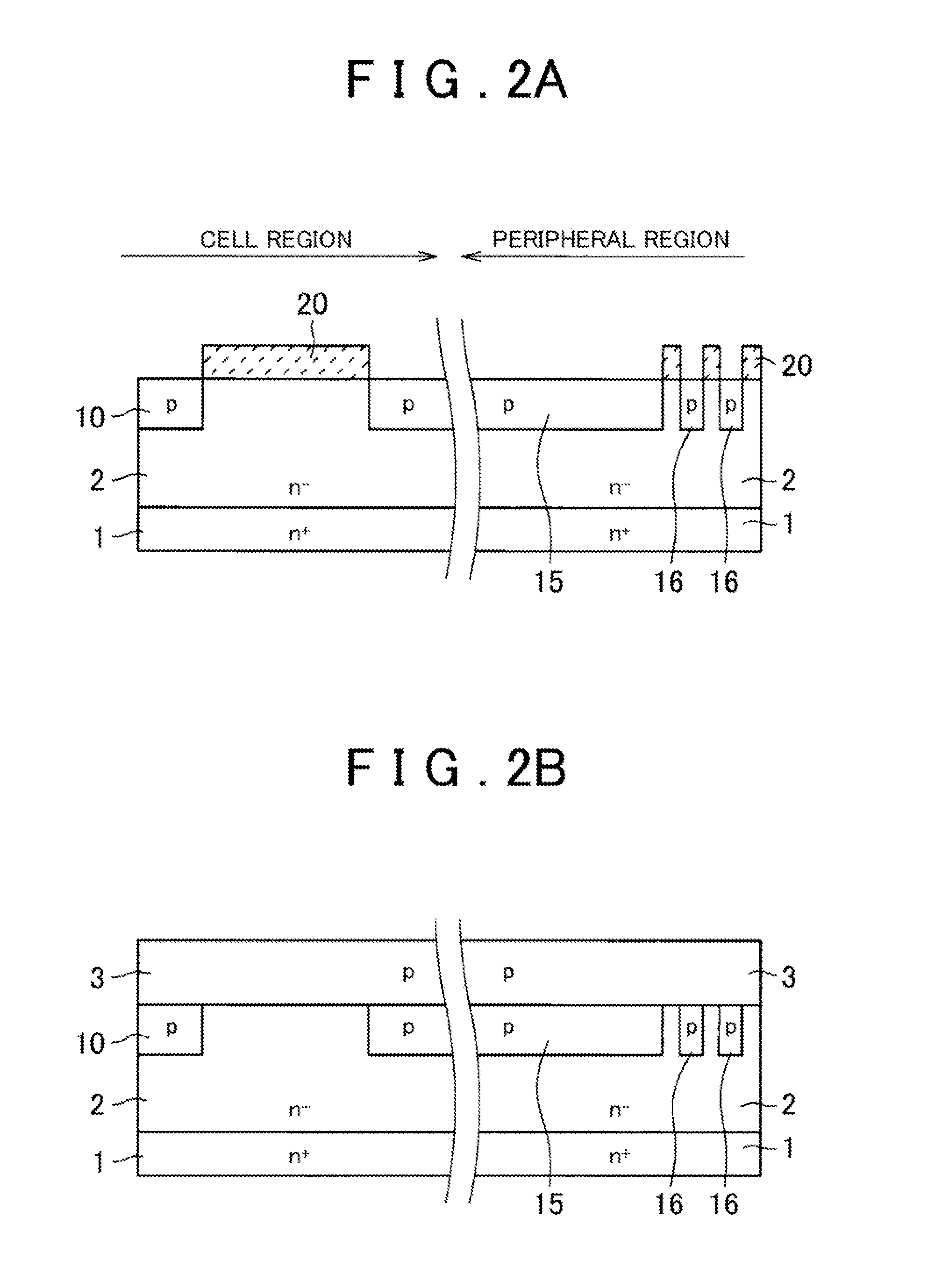
[0086]After the processes as shown in FIGS. 2A to 2D and FIGS. 3A to 3D described in the first embodiment, the processes as shown in FIGS. 6A to 6D are performed.

[0087]Specifically, in the step shown in FIG. 6A, a process similar to the step shown in FIG. 4A is performed such that the surface of the gate electrode 9 is etched back so as to be flush with the surface of the gate oxide film 8. For example, in th...


PUM


Abstract

A silicon carbide semiconductor device includes a MOSFET and a peripheral high-breakdown-voltage structure. A source region has a first recess. Trenches extend from the bottom of the first recess. A gate insulating film has an extension the shape of which follows the shape of the first recess. The surface of a gate electrode is positioned to be flush with or below the upper surface of the extension.

Description

INCORPORATION BY REFERENCE[0001]The disclosure of Japanese Patent Application No. 2014-226051 filed on Nov. 6, 2014 including the specification, drawings and abstract is incorporated herein by reference in its entirety.BACKGROUND OF THE INVENTION[0002]1. Field of the Invention[0003]The invention relates to a silicon carbide (hereinafter referred to as SiC) semiconductor device having a trench gate and a method for manufacturing the silicon carbide semiconductor device.[0004]2. Description of Related Art[0005]JP-A-2011-101036 discloses a SiC semiconductor device provided with a MOSFET having a trench gate in a cell region and a peripheral high-breakdown-voltage structure in a peripheral region surrounding the cell region.[0006]The SiC semiconductor device includes a semiconductor substrate that is composed of an n+-type SiC and is provided with an n−-type drift layer thereon. In the cell region, a p-type base region is formed in a surface portion of the n−-type drift layer, and an n+...

Claims


Application Information

Patent Timeline
IPC IPC(8): H01L29/78H01L29/66H01L29/08H01L29/06H01L29/16H01L29/10
CPCH01L29/7813H01L29/7811H01L29/1608H01L29/1095H01L29/66734H01L29/0696H01L29/063H01L29/0619H01L29/086H01L29/66068H01L29/7397H01L29/7828H01L29/0661H01L29/0869
Inventor MATSUKI, HIDEOSAKAKIBARA, JUNAOI, SACHIKOWATANABE, YUKIHIKOONOGI, ATSUSHI
Owner TOYOTA JIDOSHA KK
Why Eureka
Try Eureka