Mechanical integrity evaluation of low-k devices with bump shear

a low-k dielectric and bump shear technology, applied in semiconductor/solid-state device testing/measurement, semiconductor/solid-state device details, instruments, etc., can solve the problems of increased stress on the bond pad structure, increased mechanical integrity problems, and increased mechanical integrity of the bond pad structur

Inactive Publication Date: 2006-12-28
TAIWAN SEMICON MFG CO LTD
View PDF11 Cites 69 Cited by
  • Summary
  • Abstract
  • Description
  • Claims
  • Application Information

AI Technical Summary

Problems solved by technology

As geometries in semiconductors continue to shrink in size due to improvements in the technology for making semiconductors, the sizes of bond pad regions have become smaller, resulting in increased stress to the bond pad structure when physical connection is made to the semiconductor die.
Additional mechanical integrity problems are created by the interconnect structures used with the manufacturing smaller geometry semiconductors.
For example, bond pad structures fabricated with copper interconnect metallization and low dielectric constant (low-k) dielectri

Method used


Image

  • Mechanical integrity evaluation of low-k devices with bump shear
  • Mechanical integrity evaluation of low-k devices with bump shear
  • Mechanical integrity evaluation of low-k devices with bump shear

Examples


Embodiment Construction

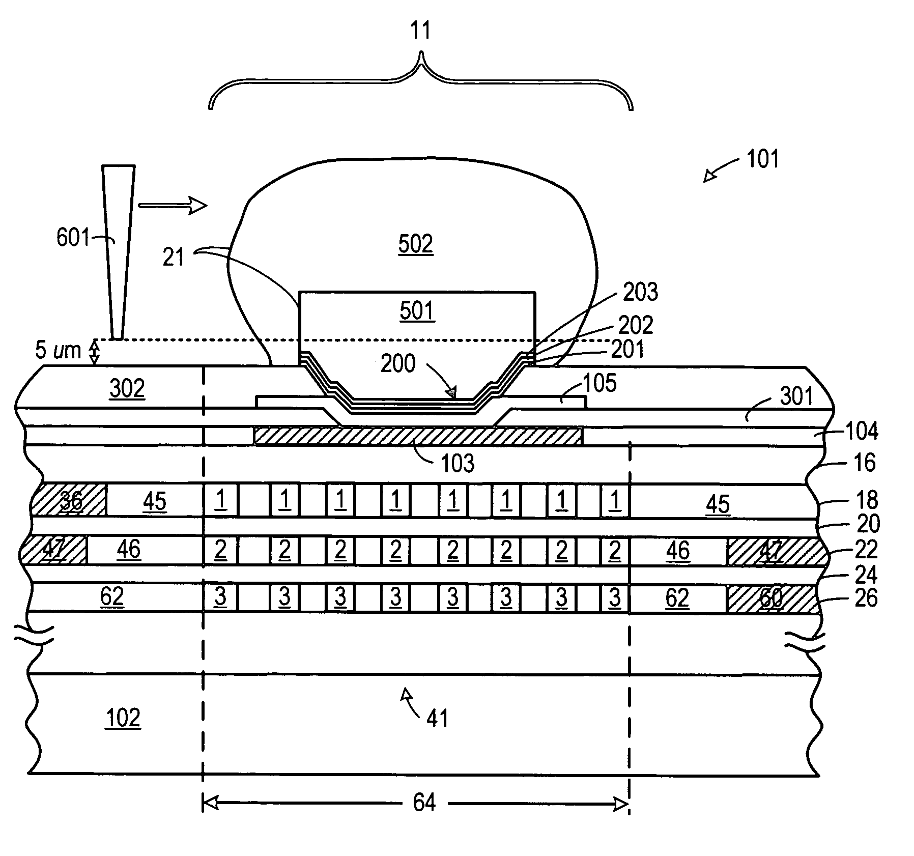
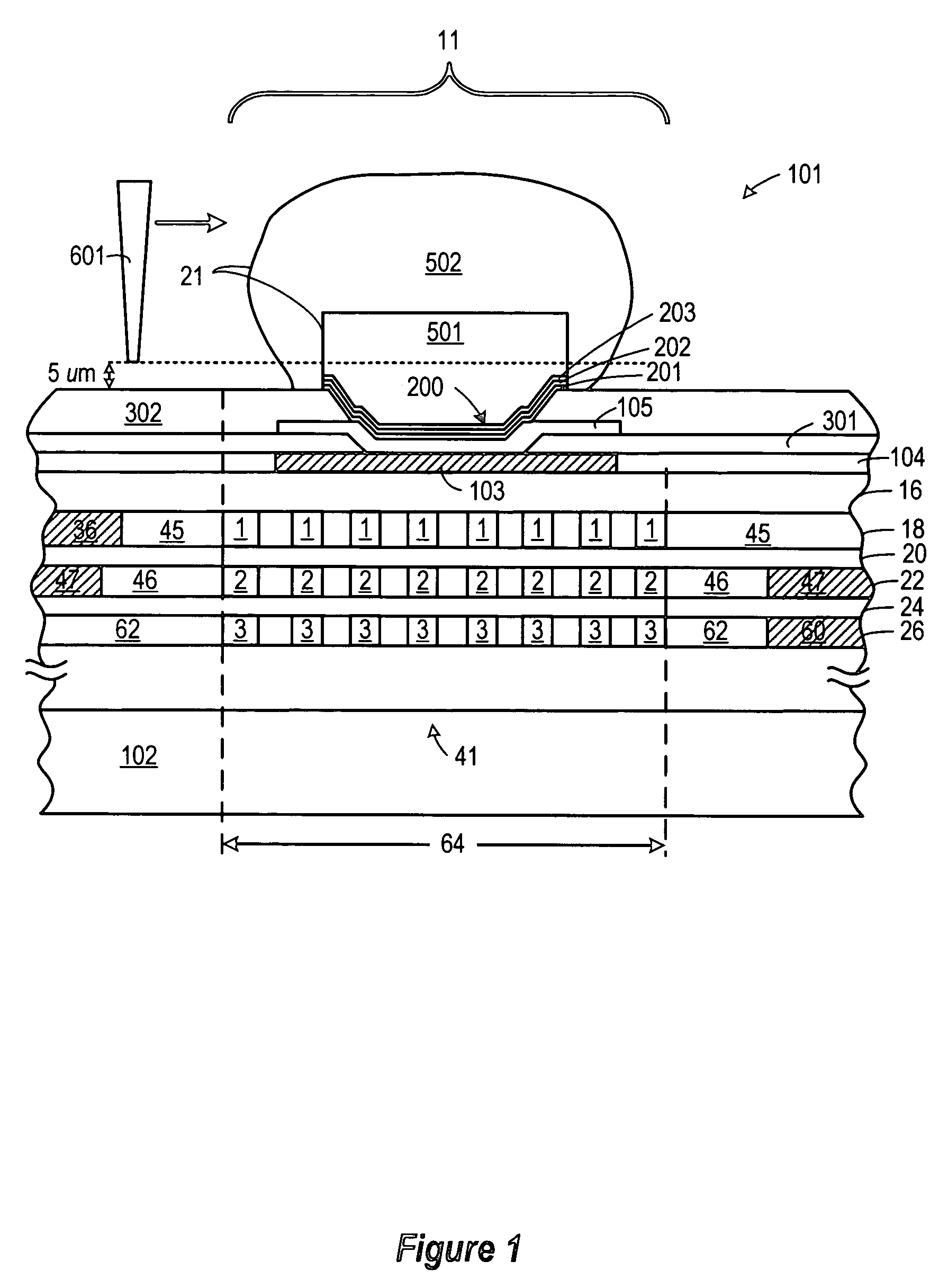
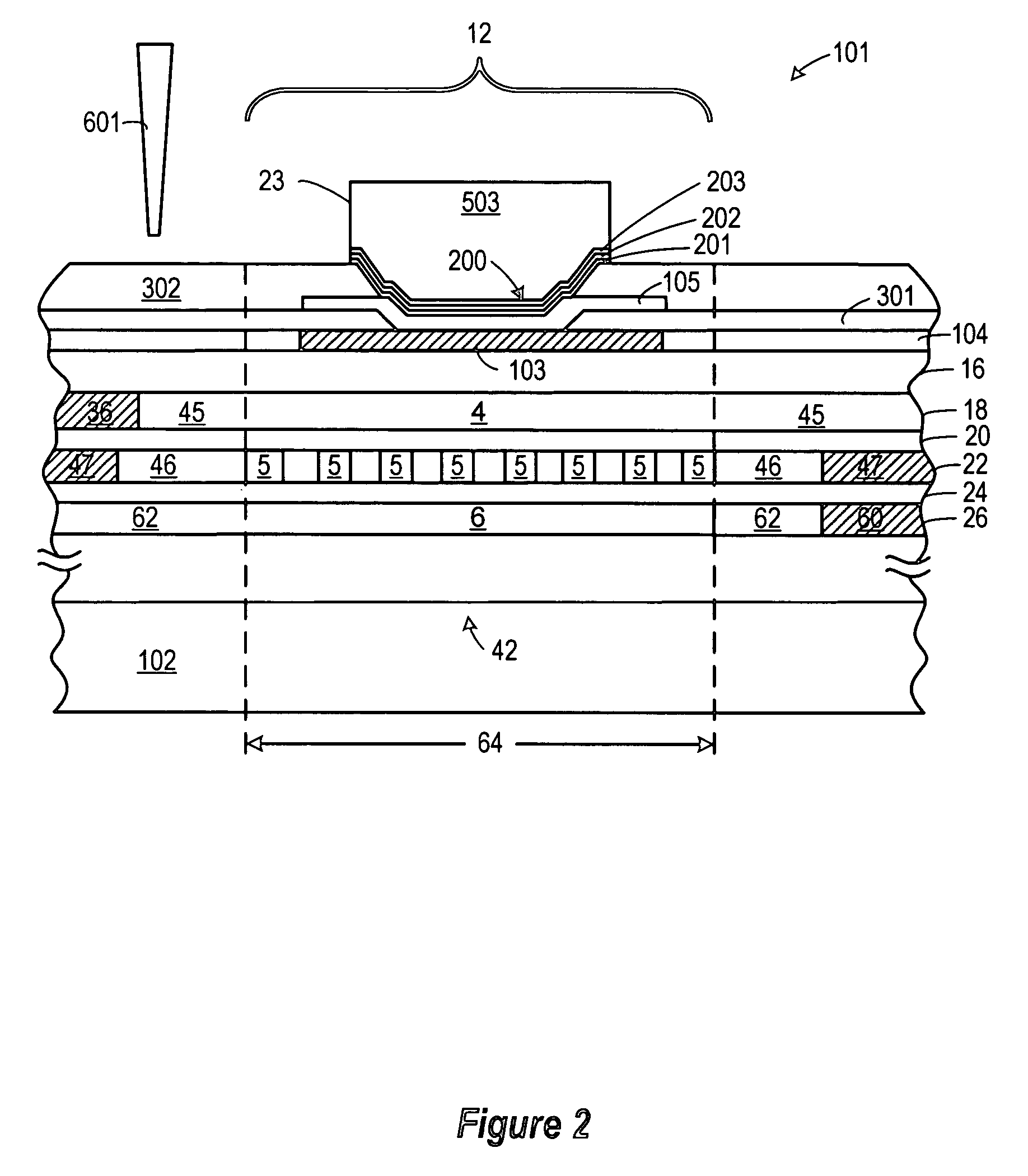
[0015] A method and apparatus are described for effectively evaluating the integration quality of integrated circuits formed with low dielectric constant (low-k) materials before die packaging occurs, such as by using an improved bond pad structure as a mechanical test feature to provide location-specific integration quality data on one or more locations on a single die. Various details are set forth in the following description, but it will be appreciated that the present invention may be practiced without these specific details, and that numerous implementation-specific decisions may be made to the invention described herein to achieve the device designer's specific goals, such as compliance with process technology or design-related constraints, which will vary from one implementation to another. While such a development effort might be complex and time-consuming, it would nevertheless be a routine undertaking for those of ordinary skill in the art having the benefit of this discl...


PUM


Abstract

A bump shear test is disclosed for evaluating the mechanical integrity of low-k interconnect stacks in an integrated circuit which includes a die test structure (11) having a stiff structural component (501, 502) positioned above and affixed to a conductive metal pad (103) formed in a last metal layer (104). The die test structure (11) may also include a dedicated support structure (41) below the conductive metal pad which includes a predetermined pattern of metal lines formed in the interconnect layers (18, 22, 26). After mounting the integrated circuit in a test device, a shear knife (601) is positioned for lateral movement to cause the shear knife to contact the stiff structural component (501). Any damage to the die test structure caused by the lateral movement of the shear knife may be assessed to evaluate the mechanical integrity of the interconnect stack.

Description

BACKGROUND OF THE INVENTION [0001] 1. Field of the Invention [0002] The present invention is directed in general to the field of semiconductor devices. In one aspect, the present invention relates to a test structure for testing integrated circuits. [0003] 2. Description of the Related Art [0004] The use of conductive balls, such as solder balls, to make electrical connection to a bond pad is a known method to make electrical connection to electrical circuitry of a semiconductor die. Conductive ball packaging is one type of semiconductor packaging known in the industry as flip chip interconnection. As geometries in semiconductors continue to shrink in size due to improvements in the technology for making semiconductors, the sizes of bond pad regions have become smaller, resulting in increased stress to the bond pad structure when physical connection is made to the semiconductor die. Additional mechanical integrity problems are created by the interconnect structures used with the man...

Claims


Application Information

Patent Timeline
IPC IPC(8): H01L21/66G01R31/26
CPCG01R31/046H01L22/12H01L22/20H01L24/05H01L2224/0401H01L2224/05084H01L2224/05624H01L2224/05647H01L2224/13006H01L2924/01013H01L2924/01014H01L2924/01022H01L2924/01029H01L2924/0105H01L2924/01073H01L2924/01074H01L2924/01078H01L2924/01082H01L2924/014H01L2924/05042H01L2924/14H01L2224/05027H01L2224/13076H01L23/3192H01L24/13H01L2224/0346H01L2224/0347H01L2224/05018H01L2224/0508H01L2224/05147H01L2224/05166H01L2224/05541H01L2224/05559H01L2224/05671H01L2224/05681H01L2224/05684H01L2224/13111H01L2224/13147H01L2224/1403H01L2224/14051H01L2224/14505H01L2924/00013H01L2924/01019H01L2924/01024H01L2924/01033H01L2924/3512H01L2224/14515H01L2224/05572H01L2224/136H01L2924/0002H01L2224/05022H01L2924/00014H01L2224/13099H01L2224/05099H01L2224/13599H01L2224/05599H01L2224/29099H01L2224/29599H01L2224/05552H01L2224/0558H01L2224/05556G01R31/70H01L2924/00012
Inventor SU, PENGPOZDER, SCOTT K.WONTOR, DAVID G.ZHAO, JIE-HUA
Owner TAIWAN SEMICON MFG CO LTD
Why Eureka
Try Eureka