Side-view light emitting diode having improved side-wall reflection structure

a technology of light-emitting diodes and side-view leds, which is applied in the direction of basic electric elements, electrical apparatus, and semiconductor devices, can solve the problems of reducing the reflective efficiency of side-view leds, increasing the number of parts and components, and complicating the work process, so as to improve light efficiency and light-emitting efficiency.

Inactive Publication Date: 2007-01-04
SAMSUNG ELECTRONICS CO LTD
View PDF4 Cites 91 Cited by
  • Summary
  • Abstract
  • Description
  • Claims
  • Application Information

AI Technical Summary

Benefits of technology

[0020] The present invention has been made to solve the foregoing problems of the prior art and therefore an object according to certain embodiments of the present invention is to provide a side-view LED having an LED window opened to a side thereof to emit light sideward, thereby enhancing light efficiency and light release efficiency.

Problems solved by technology

However, such a reflection structure entails following drawbacks.
That is, the reflective members 18a and 18b should be spaced apart from each other at a predetermined distance G. This augments the number of parts and components and complicates work process.
In addition, the conventional side-view LED experiences decrease in reflective efficiency due to light absorbed in the gap G.

Method used


Image

  • Side-view light emitting diode having improved side-wall reflection structure
  • Side-view light emitting diode having improved side-wall reflection structure
  • Side-view light emitting diode having improved side-wall reflection structure

Examples


first embodiment

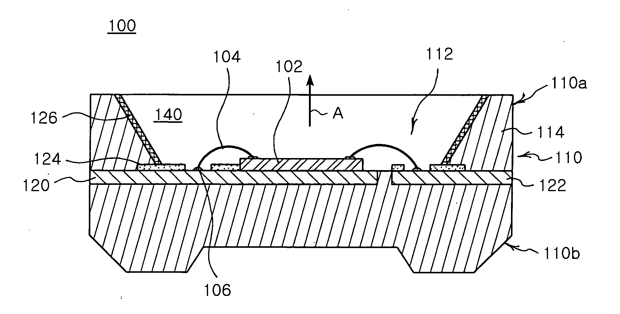
[0047] First, an explanation will be given hereunder about a side-view LED having a side-wall reflection structure of the invention with reference to FIGS. 7 and 8. FIG. 7 is a front view illustrating the side-view LED according to the invention and FIG. 8 is a cross-sectional view cut along the line VIII-VIII of FIG. 7.

[0048] As shown in FIGS. 7 and 8, the side-view LED 100 according to the first embodiment of the invention has an LED window opened to a side to emit light sideward. The side-view LED 100 is mounted in a backlight device as described above.

[0049] The side-view LED 100 includes a pair of lead frames 120 and 122, an LED chip 102, a package body 110, a high reflective metal layer 126, a transparent encapsulant 140 and an insulating layer 124. The pair of lead frames 120 and 122 each act as a terminal. The LED chip 102 is attached to a portion of the lead frames 120 and 122 and electrically connected thereto. The package body 110 houses the lead frames 120 and 122 and h...

second embodiment

[0062]FIG. 12 is a cross-sectional view of a side-view LED corresponding to FIG. 8 according to the invention.

[0063] As shown in FIG. 12, the side-view LED 200 according to the second embodiment of the invention is equal to the side view LED 100 according to the first embodiment of the invention except for an intermediate film 228 formed between a side wall 214 and a reflective layer 226. Therefore, the same components were given numeral signs that increased by 100s and will not be explained further.

[0064] The intermediate film 228 is made of an insulator selected from a group consisting of SiO2, SiN, Al2O3 and mixtures thereof. The intermediate film 228 is applied before forming of the reflective layer 226, preferably via deposition such as sputtering and electronic beam method. This allows the intermediate film 228 to have even a thickness of several □ to several μm.

[0065] The intermediate film 228 formed facilitates growth of the reflective layer 226. That is, in case where met...

third embodiment

[0067] Then, FIG. 13 is a cross-sectional view of a side-view LED corresponding to FIG. 8 according to the invention.

[0068] As shown in FIG. 13, the side-view LED 200A according to the third embodiment of the invention is equal to the side-view LED 200 except for a passivation film 230 formed on the reflective layer 226. Therefore the same components were given numeral signs that increased by 100s and will not be explained further.

[0069] The passivation film 230 formed on the reflective layer 226 is made of an insulating material selected from a group consisting of SiO2, SiN, Al2O3 and mixtures thereof like the intermediate film 228. Preferably, the passivation film 230 is disposed to a thickness of several □ to several μm via sputtering and electronic beam method.

[0070] The passivation film 230 serves to prevent debonding of the reflective layer 226. To manufacture the LED 200, a reflective layer 226 is formed and an LED chip is mounted. Then a transparent resin is poured into a ...


PUM


Abstract

The invention provides a side-view LED having an LED window opened to a side to emit light sideward. A pair of lead frames each act as a terminal. An LED chip is attached to a portion of the lead frame and electrically connected thereto. A package body houses the lead frames and has a concave formed around the LED chip. Also, a high reflective metal layer is formed integrally on a wall of the concave. A transparent encapsulant is filled in the concave to encapsulate the LED chip, while forming the LED window. In addition, an insulating layer is formed on a predetermined area of the lead frames so that the lead frames are insulated from the high reflective metal layer. The side-view LED of the invention enhances light efficiency and heat release efficiency with an improved side-wall reflection structure.

Description

CLAIM OF PRIORITY [0001] This application claims the benefit of Korean Patent Application No. 2005-59590 filed on Jul. 4, 2005 in the Korean Intellectual Property Office, the disclosure of which is incorporated herein by reference. BACKGROUND OF THE INVENTION [0002] 1. Field of the Invention [0003] The present invention relates to a side-view light emitting diode (LED) having an LED window opened to a side to emit light sideward. More particularly, the present invention relates to a side-view LED having an improved sidewall reflection structure, thereby enhancing light efficiency and heat release efficiency. [0004] 2. Description of the Related Art [0005] A liquid crystal device (LCD) mounted in monitors, mobile phones and Personal Digital Assistants (PDAs) requires external light due to absence of its own light source. Besides, the LCD generally employs a backlight device as a lighting device. The backlight device illuminates the LCD from the back, using Cold Cathode Fluorescent La...

Claims


Application Information

Patent Timeline
Patent Type & Authority Applications(United States)
IPC IPC(8): H01L33/00H01L33/60H01L33/62H01L33/64
CPCH01L33/46H01L33/486H01L33/62H01L2224/48091H01L2224/48247H01L2224/48257H01L2924/01079H01L2924/01046H01L2924/01078H01L2924/00014
Inventor KIM, HONG
Owner SAMSUNG ELECTRONICS CO LTD
Why Eureka
Try Eureka