Light-emitting diode structure and method for manufacturing the same

a technology of light-emitting diodes and diodes, which is applied in the direction of semiconductor/solid-state device manufacturing, electrical apparatus, semiconductor devices, etc., can solve the problems of low production yield, high cost, and broken holes in the insulating layer, and achieve high light efficiency and dense arrangement

Inactive Publication Date: 2013-11-07
CHI MEI LIGHTING TECH
View PDF0 Cites 43 Cited by
  • Summary
  • Abstract
  • Description
  • Claims
  • Application Information

AI Technical Summary

Benefits of technology

[0012]In one aspect, the present invention is directed to an LED structure formed by connecting a plurality of LED chips in series and has the advantages such as dense arrangement and high light efficiency.
[0013]In another aspect, the present invention is directed to an LED structure and a method for manufacturing the same, in which a reflective insulating layer covers an interconnection layer, a mesa structure and an exposed portion of a first conductivity type semiconductor layer, so as to perform packaging in a flip chip manner, thereby achieving the efficacies such as high heat dissipation, being free of wire bonding, and low thermal resistance.
[0014]In yet another aspect, the present invention is directed to an LED structure and a method for manufacturing the same, in which an interconnection layer extends, from an exposed portion of a first conductivity type semiconductor layer of one of adjacent LED chips, directly through the side of the mesa structure of another adjacent LED chip, and onto the mesa structure. Therefore, the aspect ratio of an interconnection layer can be significantly reduced, thereby effectively enhancing the step coverage capability during the deposition of the interconnection layer and further avoiding the occurrence of disconnections during the deposition of the interconnection layer.

Problems solved by technology

As a wire bonding manner has the problems of high cost and a low production yield, it is further developed to connect a plurality of LED chips in series by embedding a metal.
Therefore, the aspect ratio of the isolation trench 122 is too high, the material of the insulating layer 124 cannot be filled easily, and discontinuous deposition occurs easily, which easily causes broken holes in the insulating layer 124.
Therefore, the production yield of the serially connected LED structure 100 is undesirable.
Therefore, the production yield of such a serially connected LED structure 100 is undesirable.
Therefore, a heretofore unaddressed need exists in the art to address the aforementioned deficiencies and inadequacies.

Method used


Image

  • Light-emitting diode structure and method for manufacturing the same
  • Light-emitting diode structure and method for manufacturing the same
  • Light-emitting diode structure and method for manufacturing the same

Examples


Embodiment Construction

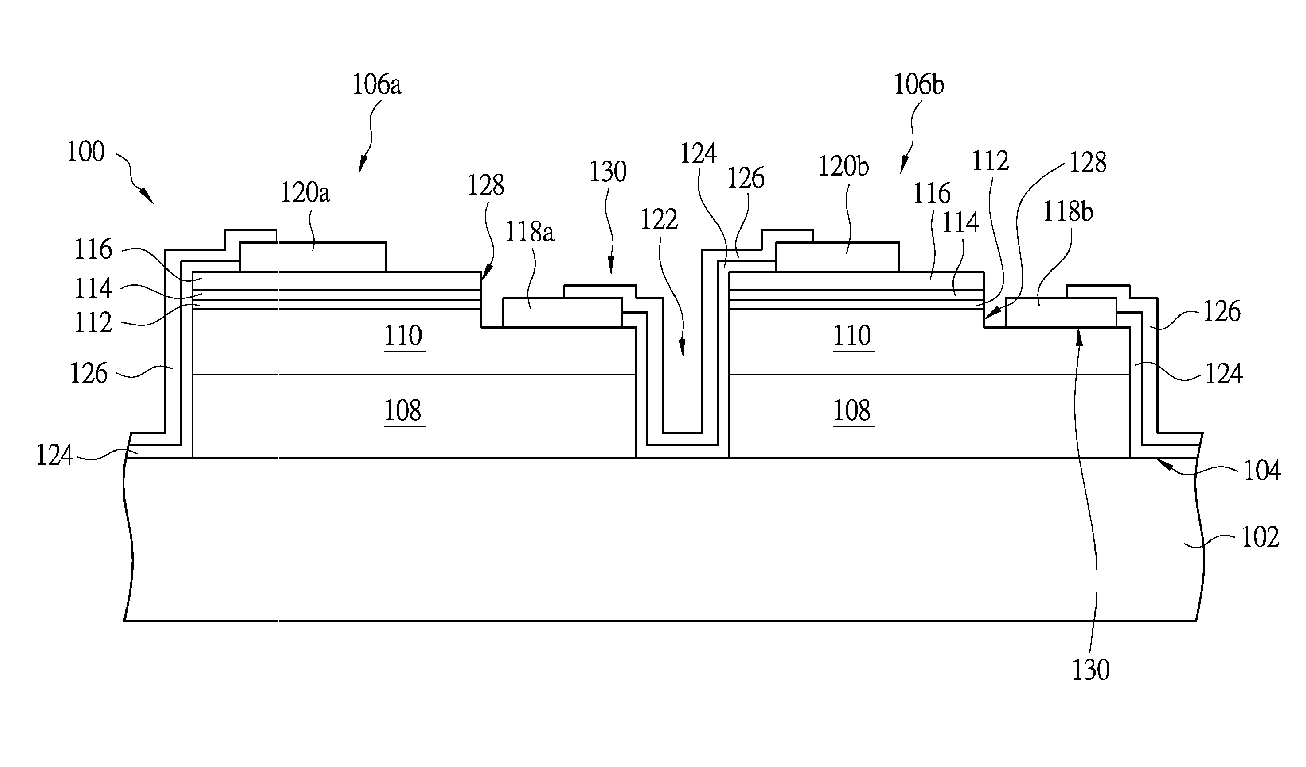
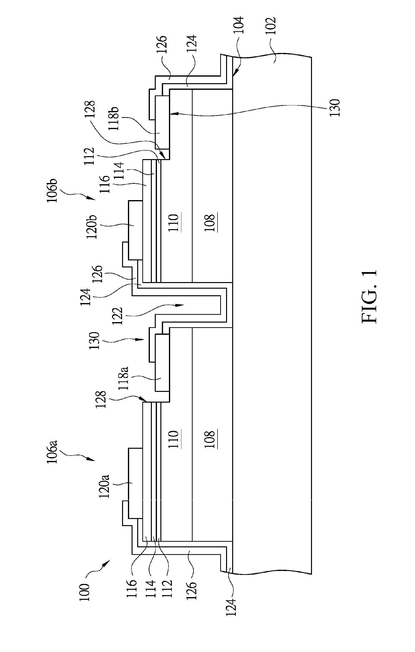
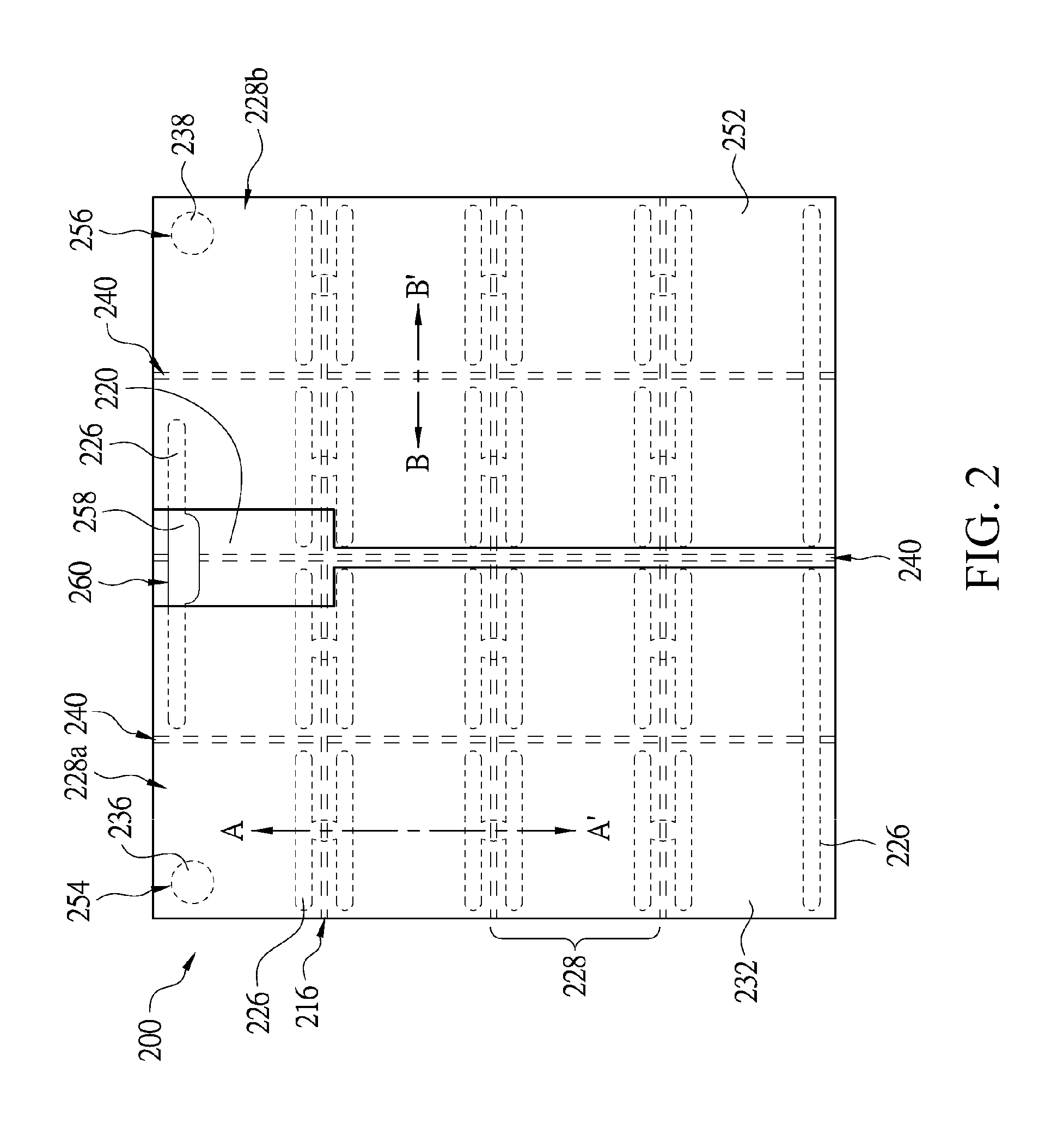
[0053]The present invention will now be described more fully hereinafter with reference to the accompanying drawings, in which exemplary embodiments of the invention are shown. This invention may, however, be embodied in many different forms and should not be construed as limited to the embodiments set forth herein. Rather, these embodiments are provided so that this disclosure will be thorough and complete, and will fully convey the scope of the invention to those skilled in the art. Like reference numerals refer to like elements throughout.

[0054]Example embodiments are described herein with reference to cross-sectional illustrations that are schematic illustrations of idealized embodiments (and intermediate structures) of example embodiments. As such, variations from the shapes of the illustrations as a result, for example, of manufacturing techniques and / or tolerances, are to be expected. Thus, example embodiments should not be construed as limited to the shapes of regions illust...


PUM


Abstract

A light-emitting diode (LED) structure includes an insulation substrate; LED chips each includes an epitaxial layer having a first conductivity type semiconductor layer, an active layer, and a second conductivity type semiconductor layer stacked on the insulation substrate, and comprises a mesa structure and an exposed portion of the first conductivity type semiconductor layer adjacent to each other, and a first isolation trench within the mesa structure; interconnection layers connect the LED chips; electrode pads respectively connected to exposed portions of the semiconductor layers; a reflective insulating layer covering the interconnection layers, the mesa structures and the electrode pads, and having penetration holes respectively exposing a portion of the electrode pads; and bonding pads located on a portion of the reflective insulating layer and connected to the electrode pads through the penetrating holes. A method of manufacturing the LED structure.

Description

CROSS-REFERENCE TO RELATED APPLICATIONS[0001]This non-provisional application claims priority under 35 U.S.C. §119(a) on Patent Application Nos. 101116039 filed in Taiwan, R.O.C. on May 4, 2012, 101128042 filed in Taiwan, R.O.C. on Aug. 3, 2012, and 102113113 filed in Taiwan, R.O.C. on Apr. 12, 2013, the entire contents of which are hereby incorporated by reference.FIELD OF THE INVENTION[0002]The present invention relates to a light-emitting structure, and more particularly to a light-emitting diode (LED) structure and a method for manufacturing the same.BACKGROUND OF THE INVENTION[0003]Nowadays, to enhance the overall light emission efficiency of an LED, it is developed to connecting a plurality of LED chips in series in a wire bonding manner. As a wire bonding manner has the problems of high cost and a low production yield, it is further developed to connect a plurality of LED chips in series by embedding a metal.[0004]FIG. 1 is a partial sectional view of a conventional serially-...

Claims


Application Information

Patent Timeline
Patent Type & Authority Applications(United States)
IPC IPC(8): H01L33/08
CPCH01L33/08H01L27/156H01L33/46H01L33/62H01L2924/0002H01L2924/00
Inventor LEE, HSUEH LINCHU, CHANG HSINCHEN, YUAN TZEHSU, CHIH KUEI
Owner CHI MEI LIGHTING TECH
Why Eureka
Try Eureka