
Technique to write to a non-volatile memory

a non-volatile memory and writing technology, applied in the direction of memory architecture accessing/allocation, instruments, computing, etc., can solve the problem that the cells of flash memory typically cannot be re-written without first being erased

Active Publication Date: 2007-01-04
SK HYNIX NAND PROD SOLUTIONS CORP
View PDF7 Cites 126 Cited by
  • Summary
  • Abstract
  • Description
  • Claims
  • Application Information

AI Technical Summary

Problems solved by technology

Although a typical flash memory has a significantly faster access time than a magnetic storage device, unlike the magnetic storage device, the cells of the flash memory typically cannot be re-written without first being erased.

Method used


Image

  • Technique to write to a non-volatile memory
  • Technique to write to a non-volatile memory
  • Technique to write to a non-volatile memory

Examples


Embodiment Construction

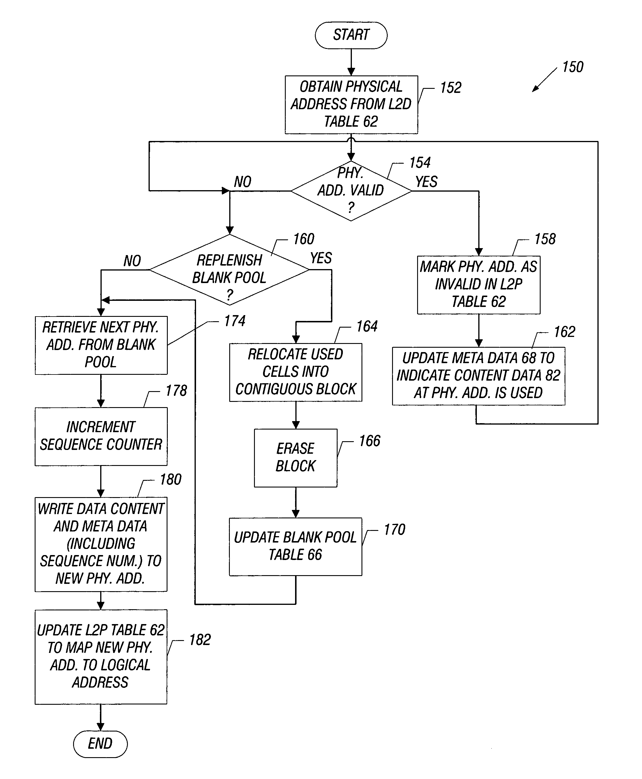
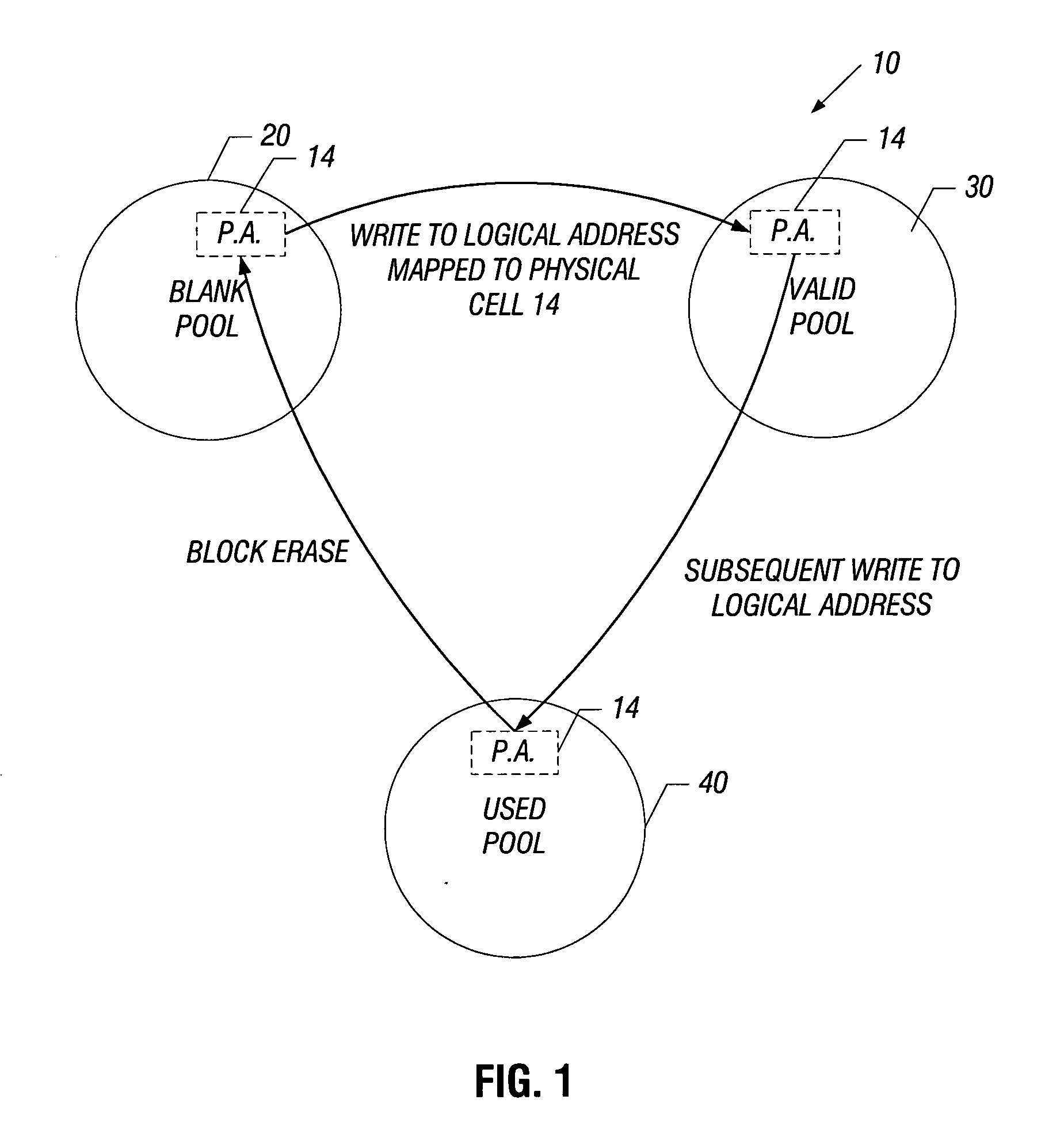
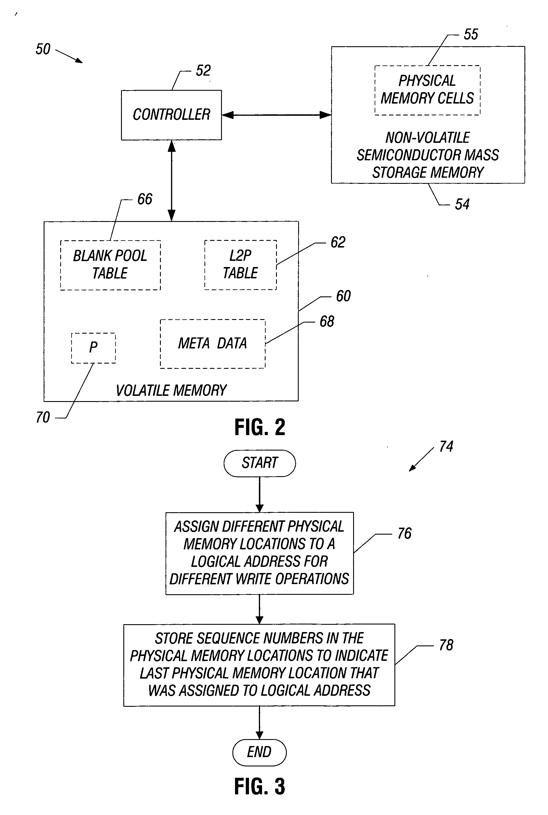
[0015] In accordance with embodiments of the invention described herein, dynamic addressing is used in connection with a non-volatile semiconductor memory (herein called a “non-volatile memory”) for purposes of minimizing the write latency of the memory. More specifically, in accordance with embodiments of the invention that are described herein, the non-volatile memory is, from a software standpoint, addressed using logical addresses. From the standpoint of the physical read and write operations that are performed with the memory, the dynamic addressing translates, or maps, the logical addresses to physical addresses of the memory. The dynamic addressing continually changes the mapping between the logical and physical addresses to ensure that each logical write operation causes data to be stored in a previously erased location (i.e., at a different physical address) of the non-volatile memory. Thus, with dynamic addressing, each logical write operation produces a single operation. ...


PUM


Abstract

A technique includes performing a plurality of write operations to store data in different physical memory locations. Each of the physical memory locations are associated with a logical address that is shared in common among the physical addresses. The technique includes storing sequence information in the physical memory locations to indicate which one of the write operations occurred last.

Description

BACKGROUND [0001] The invention generally relates to a technique to write to a non-volatile memory. [0002] Non-volatile semiconductor memories, such as flash memories, are attractive for applications in which data is to be preserved in the event of a normal system shutdown / hibernation or power failure. Thus, a memory that is formed from flash memory devices may be used to store data in a disk cache or a solid state disk. Although a typical flash memory has a significantly faster access time than a magnetic storage device, unlike the magnetic storage device, the cells of the flash memory typically cannot be re-written without first being erased. [0003] As a more specific example, before a bit of data is stored in a conventional flash memory cell, the cell is first erased. In this erased state, the cell is indicative of a particular logic state, such as a logic “one” state, for example. In a subsequent write operation to the flash memory cell, if a logic one is to be stored in the cel...

Claims


Application Information

Patent Timeline
IPC IPC(8): G06F12/00
CPCG06F2212/7209G06F12/0246
Inventor TRIKA, SANJEEV N.FABER, ROBERT W.COULSON, RICKMATTHEWS, JEANNA N.
Owner SK HYNIX NAND PROD SOLUTIONS CORP
Features
  • Generate Ideas
  • Intellectual Property
  • Life Sciences
  • Materials
  • Tech Scout
  • Unparalleled Data Quality
  • Higher Quality Content
  • 60% Fewer Hallucinations
Learn More