Optical element, in particular for an objective or an illumination system of a microlithographic projection exposure apparatus

a technology of exposure apparatus and optical element, which is applied in the field of optical element, can solve the problems of telecentry errors and contrast loss, and increase the difficulty of optical imaging, and achieve the effect of improving imaging quality

Inactive Publication Date: 2007-01-11
CARL ZEISS SMT GMBH
View PDF4 Cites 16 Cited by
  • Summary
  • Abstract
  • Description
  • Claims
  • Application Information

AI Technical Summary

Benefits of technology

[0008] The object of the present invention is to provide an optical element, in particular for an objective or an illumination system of a microlithographic projection exposu...

Problems solved by technology

It is known that, in the case of single-crystalline cubic materials such as for example calcium fluoride which is used in microlithography in particular at working wavelengths of less than 250 nm, in spite of the high level of symmetry present in the crys...

Method used


Image

  • Optical element, in particular for an objective or an illumination system of a microlithographic projection exposure apparatus
  • Optical element, in particular for an objective or an illumination system of a microlithographic projection exposure apparatus
  • Optical element, in particular for an objective or an illumination system of a microlithographic projection exposure apparatus

Examples


Embodiment Construction

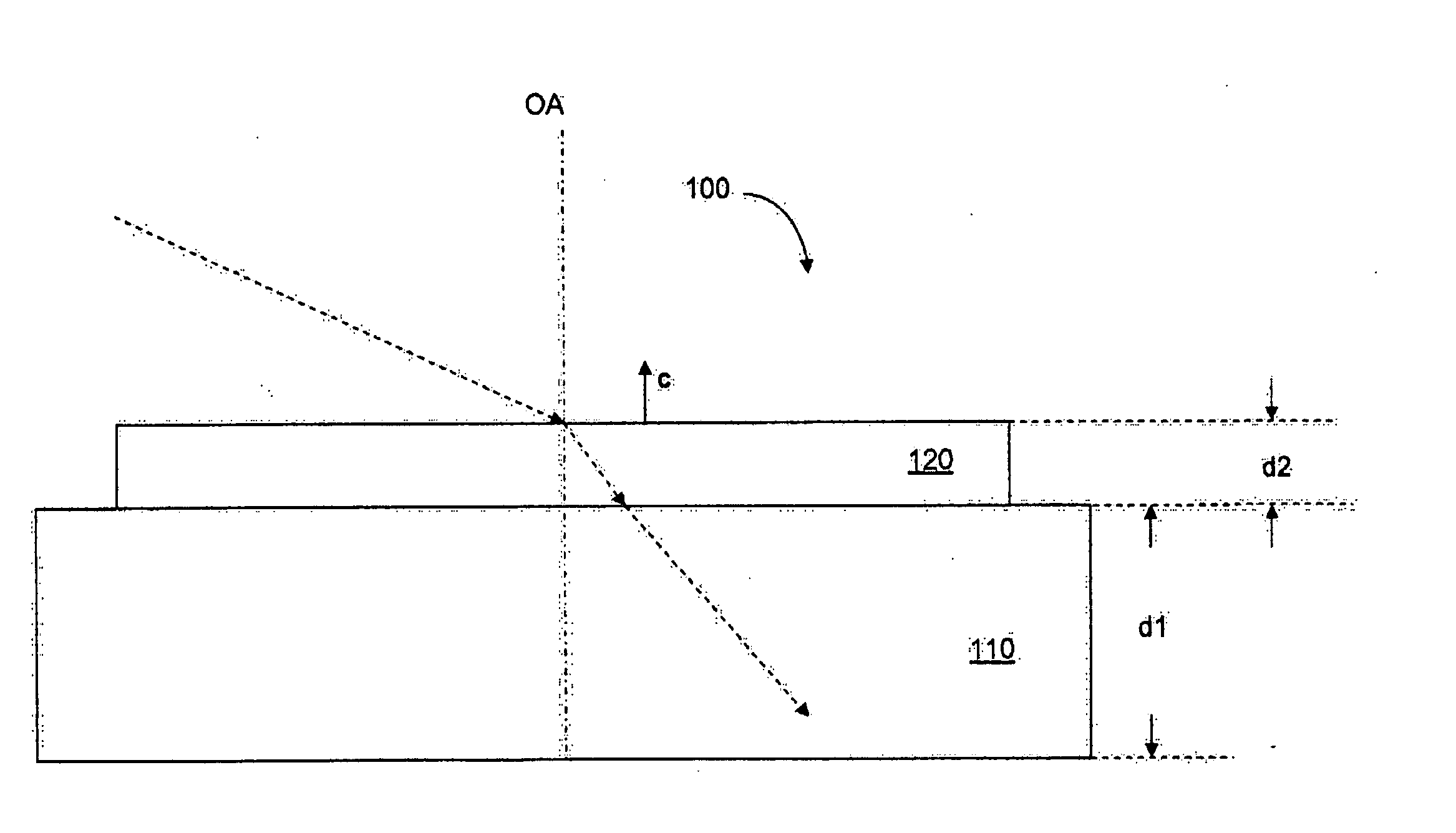
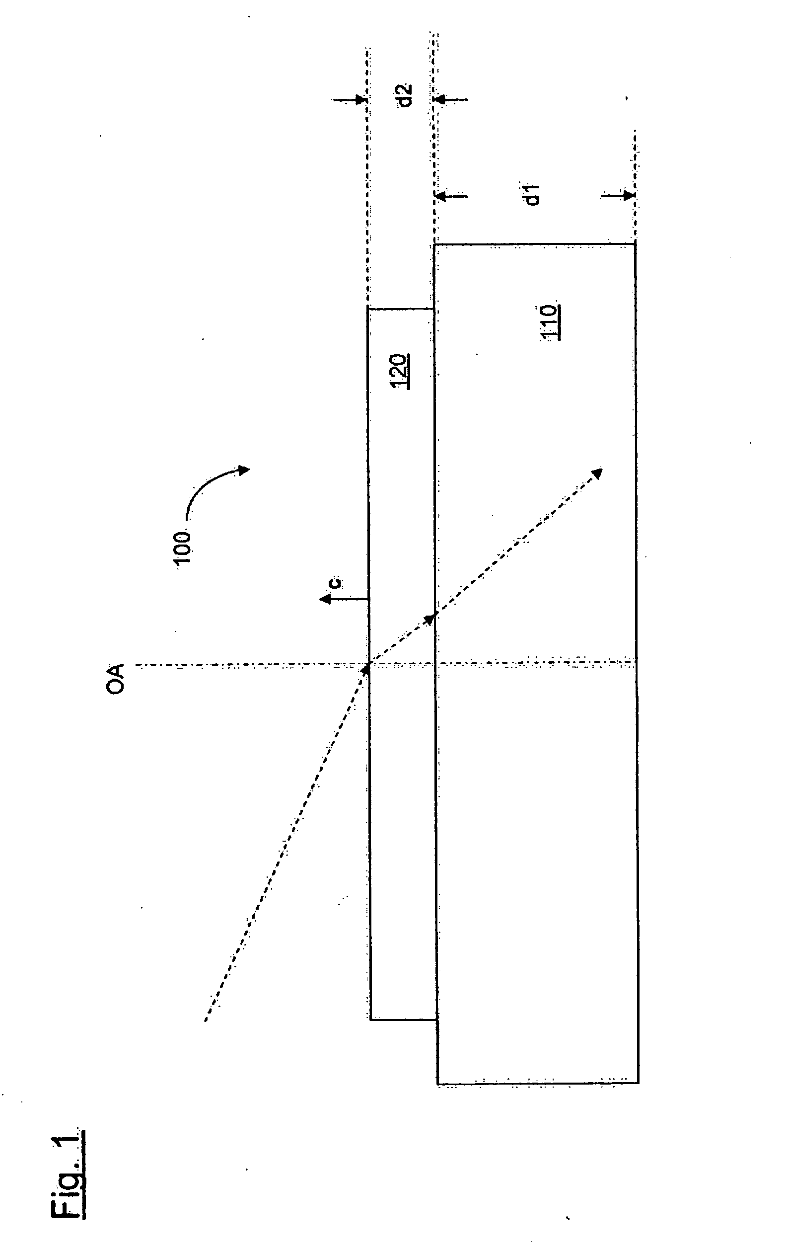
[0043]FIG. 1 is a diagrammatic view, not true to scale, showing the structure of an optical element 100 according to a first preferred embodiment of the invention.

[0044] The optical element 100 includes a substrate 110 in the form of a plane-parallel plate of calcium fluoride, which is of a thickness d1 and which is produced in a (111)-orientation, that is to say the axis EA of the element is perpendicular to the {111}-crystal plane and thus parallel to the -crystal direction of the substrate 110. The diameter of the plane-parallel plate is of any desired value and can be for example 20 cm. The thickness d1 is also basically of any desired value and in the illustrated embodiment can be assumed to be d1=2 cm.

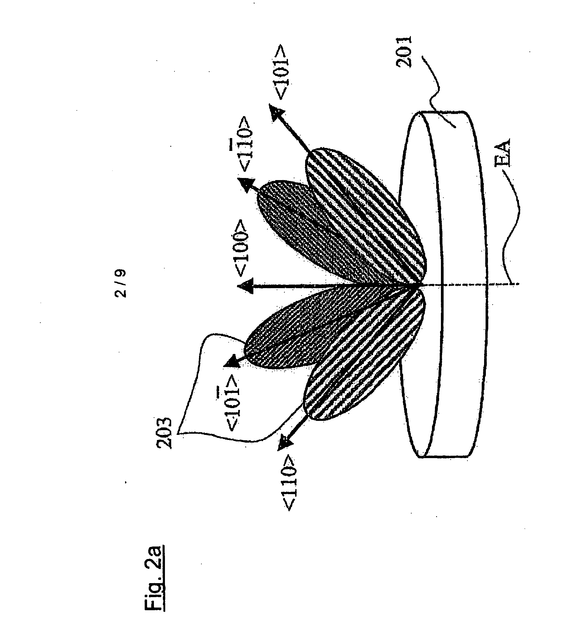
[0045] A layer 120 of lanthanum fluoride is applied to the substrate 110. The layer 120 is grown in a defined manner and in crystalline form so that the optical crystal axis in the hexagonal crystal structure of the lanthanum fluoride material, referred usually and also hereina...


PUM


Abstract

The invention concerns an optical element, in particular for an objective or an illumination system of a microlithographic projection exposure apparatus, including a substrate which for light of a predetermined working wavelength which passes through the substrate causes a first retardation between mutually perpendicular polarization states, and a layer which is epitaxially grown on the substrate and which is made from a material with non-cubic crystal structure, which by virtue of natural birefringence causes a second retardation between mutually perpendicular polarization states, which at least partially compensates for the first retardation caused in the substrate.

Description

CROSS-REFERENCE TO RELATED APPLICATION [0001] Under 35 U.S.C. §119, this application claims priority to German Patent Application No. 10 2005 021 340.5, filed May 4, 2005, the contents of which are hereby incorporated by reference. BACKGROUND OF THE INVENTION [0002] 1. Field of the Invention [0003] The invention concerns an optical element, in particular for an objective or an illumination system of a microlithographic projection exposure apparatus. [0004] 2. Description of the Related Art [0005] It is known that, in the case of single-crystalline cubic materials such as for example calcium fluoride which is used in microlithography in particular at working wavelengths of less than 250 nm, in spite of the high level of symmetry present in the crystal structure, the effect of what is referred to as intrinsic birefringence occurs, which at the high levels of resolution required in microlithography, results in telecentry errors and losses in contrast and thus causes increased difficult...

Claims


Application Information

Patent Timeline
IPC IPC(8): C09K19/52
CPCG02B1/02G03F7/70966G02B27/281G02B5/3083
Inventor MUELLER, RALFDITTMANN, OLAFTOTZECK, MICHAELKRAEHMER, DANIELZACZEK, CHRISTOPHSCHUSTER, KARL-HEINZ
Owner CARL ZEISS SMT GMBH
Why Eureka
Try Eureka