White light emitting device

a light-emitting device and white light technology, applied in the direction of semiconductor devices, basic electric elements, electrical equipment, etc., can solve the problem that the recombination efficiency of the first active region emitting short wavelength cannot be boosted sufficiently, and achieve the effect of enhancing the recombination efficiency of the active region emitting short wavelength

Inactive Publication Date: 2007-01-11
SAMSUNG ELECTRO MECHANICS CO LTD
View PDF6 Cites 13 Cited by
  • Summary
  • Abstract
  • Description
  • Claims
  • Application Information

AI Technical Summary

Benefits of technology

[0015] The present invention has been made to solve the foregoing problems of the prior art and it is therefore an object of the present invention to provide a novel monolithic light emitting device which enhances recombination efficiency of short wavelength active region by realizing long wavelength active region out of a plurality of active regions emitting different wavelength with a discontinuous structure such as quantum dots or quantum crystallites, instead of a continuous layer structure.
[0017] According to present invention, the second active region emitting long wavelength which induces constraint of carriers has the discontinuous structure comprising quantum dots or crystallites. This substantially enhances efficiency of carriers injection provided to the first active region emitting short wavelength.

Problems solved by technology

If the total area of the quantum well structure is less than 20%, sufficient brightness cannot be ensured, while if it is greater than 75%, recombination efficiency of the first active region emitting short wavelength cannot be boosted sufficiently.

Method used


Image

  • White light emitting device
  • White light emitting device
  • White light emitting device

Examples


Embodiment Construction

[0033] Preferred embodiments of the present invention will now be described in detail with reference to the accompanying drawings.

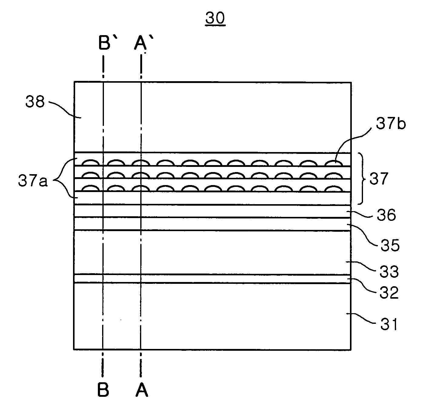
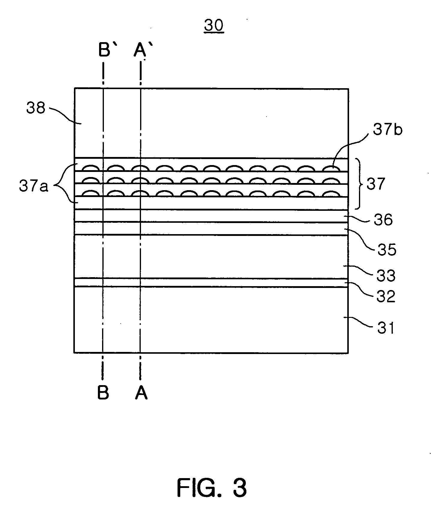
[0034]FIG. 3 is a sectional view of a white light emitting device of the invention.

[0035] Referring to FIG. 3, the white light emitting device 30 includes a first conductivity type nitride layer 33 and a second conductivity type nitride layer 38 formed on a substrate 31 having a buffer layer 32 interposed between the substrate 31 and the first conductivity type nitride layer 33, and active regions 35,36,37 emitting blue, green and red wavelength lights between the first and second conductivity type nitride layers 33, 38.

[0036] The blue and green active regions 35,36 include typical continuous layers, and may include a multiple quantum well structure having a plurality of quantum well layers and quantum barrier layers (not illustrated). Also, the blue and green active regions 35,36 may have quantum well layers, one emitting light of about 450 to 475 nm ...


PUM


Abstract

The invention relates to a nitride light emitting device including first and second conductivity type nitride layers and a plurality of active regions emitting light of different wavelength. The active regions are sequentially formed between the first and the second conductivity type nitride layers. The active regions include at least one first active region having a plurality of first quantum barrier layers and quantum well layers, and a second active region emitting light of a wavelength larger than that of the first active region. The second active region has a plurality of second quantum barrier layers and at least one discontinuous quantum well structure formed between the plurality of second quantum barrier layers. The discontinuous quantum well structure comprises a plurality of quantum dots or crystallites.

Description

CLAIM OF PRIORITY [0001] This application claims the benefit of Korean Patent Application No. 2005-61101 filed on Jul. 7, 2005, in the Korean Intellectual Property Office, the disclosure of which is incorporated herein by reference. BACKGROUND OF THE INVENTION [0002] 1. Field of the Invention [0003] The present invention relates to a white light emitting device. More particularly, the present invention relates to a monolithic white light emitting device which has at least 2 active regions emitting light of different wavelength configured as a single device, and a manufacturing thereof. [0004] 2. Description of the Related Art [0005] In general, a white light emitting device employing Light Emitting Diode (LED) ensures high brightness and high efficiency, thus widely used as a back light for lighting apparatus or display apparatus. [0006] Broadly known methods for configuring the white light emitting device include simple combination of blue, red and green LEDs manufactured as a sepa...

Claims


Application Information

Patent Timeline
Patent Type & Authority Applications(United States)
IPC IPC(8): H01L33/00H01L33/06H01L33/32
CPCH01L33/06H01L33/32H01L33/08
Inventor KIM, MIN HOMIN, KYEONG IKKOIKE, MASAYOSHI
Owner SAMSUNG ELECTRO MECHANICS CO LTD
Why Eureka
Try Eureka