Vertical structure nonpolar LED chip on lithium gallate substrate and preparation method therefor

a non-polar, led chip technology, applied in the direction of basic electric elements, electrical equipment, semiconductor devices, etc., can solve the problems of difficult improvement of the light effect of the horizontal structure led, increase the cost, and reduce the yield, so as to facilitate the preparation of the vertical structure led chip. , good electric conductivity

Active Publication Date: 2019-07-04
SOUTH CHINA UNIV OF TECH
View PDF0 Cites 5 Cited by
  • Summary
  • Abstract
  • Description
  • Claims
  • Application Information

AI Technical Summary

Benefits of technology

[0028](1) The present invention uses lithium gallate as a substrate, which has good electric conduct

Problems solved by technology

However, due to the bottleneck suppression effect on the current in the horizontal direction, the light effect of the horizontal structure LED is difficult to be improved.
However, a vertical structure LED chip on the sapphire substr

Method used


Image

  • Vertical structure nonpolar LED chip on lithium gallate substrate and preparation method therefor

Examples


example 1

[0035]The preparation method for the vertical structure nonpolar LED chip on the lithium gallate substrate comprises the following steps:

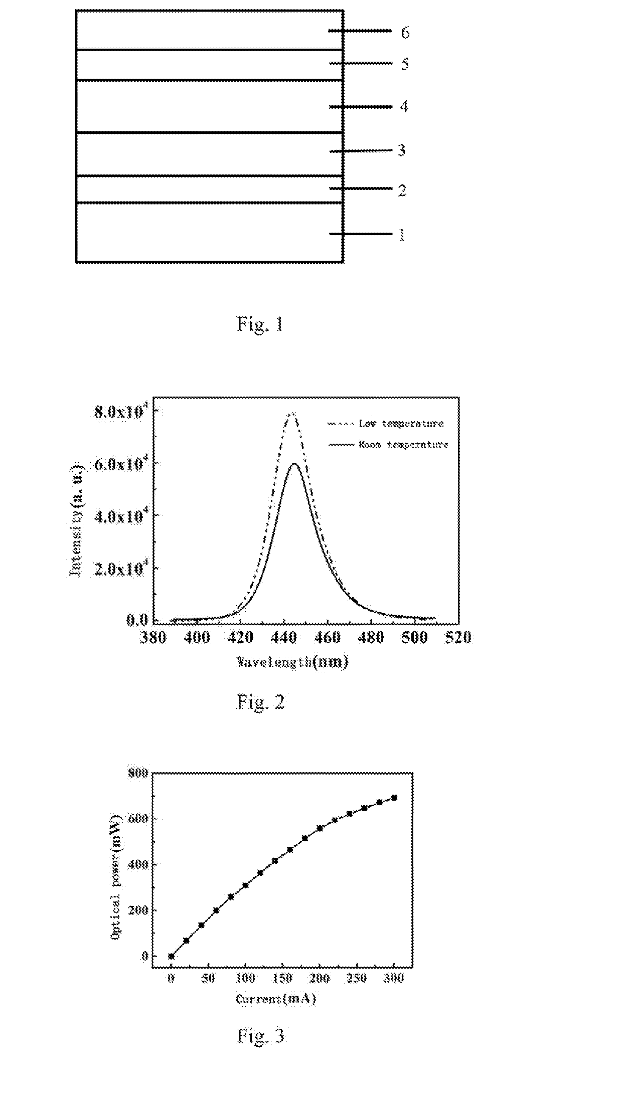
[0036](1) A pulsed laser deposition process is used to grow LED epitaxial wafers on a lithium gallate substrate, wherein the LED epitaxial wafers comprise a GaN buffer layer grown on the lithium gallate substrate, a non-doped GaN layer on the GaN buffer layer, an n-type Si-doped GaN thin film on the non-doped GaN layer with a doping concentration of 1.0×109 cm−3, an InGaN / GaN quantum well on the n-type doped GaN thin film, and a p-type Mg-doped GaN thin film on the InGaN / GaN quantum well with a doping concentration of 1.0×1017 cm−3. The lithium gallate substrate has a (100) plane as an epitaxial surface. The GaN buffer layer has a thickness of 30 nm; the non-doped GaN layer has a thickness of 100 nm; the n-type Si-doped GaN film has a thickness of 1 m; the InGaN / GaN quantum well is an InGaN well layer / a GaN barrier layer of 10 cycles, wherein the I...

example 2

[0045]The preparation method for the vertical structure nonpolar LED chip on the lithium gallate substrate comprises the following steps:

[0046](1) A pulsed laser deposition process is used to grow LED epitaxial wafers on a lithium gallate substrate, wherein the LED epitaxial wafers comprise a GaN buffer layer grown on the lithium gallate substrate, a non-doped GaN layer on the GaN buffer layer, an n-type Si-doped GaN thin film on the non-doped GaN layer with a doping concentration of 3.0.0×1019 cm−3, an InGaN / GaN quantum well on the n-type Si-doped GaN thin film, and a p-type Mg-doped GaN thin film on the InGaN / GaN quantum well with a doping concentration of 3.0×1017 cm−3. The lithium gallate substrate has a (100) plane as an epitaxial surface. The GaN buffer layer has a thickness of 60 nm; the non-doped GaN layer has a thickness of 200 nm; the n-type Si-doped GaN film has a thickness of 2 m; the InGaN / GaN quantum well is an InGaN well layer / a GaN barrier layer of 7 cycles, wherein ...

example 3

[0054]The preparation method for the vertical structure nonpolar LED chip on the lithium gallate substrate comprises the following steps:

[0055](1) A pulsed laser deposition process is used to grow LED epitaxial wafers on a lithium gallate substrate, wherein the LED epitaxial wafers comprise a GaN buffer layer grown on the lithium gallate substrate, a non-doped GaN layer on the GaN buffer layer, an n-type Si-doped GaN thin film on the non-doped GaN layer with a doping concentration of 5.0.0×109 cm−3, an InGaN / GaN quantum well on the n-type Si-doped GaN thin film, and a p-type Mg-doped GaN thin film on the InGaN / GaN quantum well with a doping concentration of 5.0.0×1017 cm−3. The lithium gallate substrate has a (100) plane as an epitaxial surface. The GaN buffer layer has a thickness of 90 nm; the non-doped GaN layer has a thickness of 300 nm; the n-type Si-doped GaN film has a thickness of 3 μm; the InGaN / GaN quantum well is an InGaN well layer / a GaN barrier layer of 7 cycles, wherei...


PUM


Abstract

The present invention discloses a vertical structure nonpolar LED chip on a lithium gallate substrate and a preparation method therefor. According to the method, LED epitaxial wafers are grown on a lithium gallate substrate, wherein the LED epitaxial wafers comprise a GaN buffer layer grown on the lithium gallate substrate, a non-doped GaN layer on the GaN buffer layer, an n-type doped GaN thin film on the non-doped GaN layer, an InGaN/GaN quantum well on the n-type doped GaN thin film and a p-type doped GaN thin film on the InGaN/GaN quantum well. Then, electrode patterns are prepared on the surfaces of the LED epitaxial wafers by the steps of spin coating, photoetching, developing and cleaning, and an electrode metal is sequentially deposited on the upper surfaces of the epitaxial wafers. Then, the LED epitaxial wafers are transferred to a copper substrate. Then, the original lithium gallate substrate is lifted off by an HCl solution, a silicon dioxide protective layer is prepared, and the corresponding part of an electrode is exposed. Then, SiO2 on the electrode is etched away, and a complete vertical structure LED chip is formed.

Description

FIELD OF THE INVENTION[0001]The present invention relates to the field of vertical structure LED chips, in particular to a vertical structure nonpolar LED chip on a lithium gallate (LiGaO2) substrate and a preparation method therefor.BACKGROUND OF THE INVENTION[0002]As a new type of solid illumination source and environmentally friendly light source, a light-emitting diode (LED) has the characteristics of small size, low power consumption, environmental protection, long service life, high brightness, low heat and colorfulness, etc., and has a wide range of applications in outdoor lighting, commercial lighting, decorative engineering and other fields.[0003]At present, most of the industrialized LEDs use sapphire as the substrate; however, since the sapphire itself is not electrically conductive, the current flow direction of the prepared LED chip is horizontal, that is, the prepared LED chip is a horizontal structure LED. The horizontal structure LED has been widely used due to its s...

Claims


Application Information

Patent Timeline
IPC IPC(8): H01L33/00H01L33/06H01L33/32H01L33/12
CPCH01L33/007H01L33/06H01L33/32H01L33/12H01L2933/0016H01L2933/0025H01L33/005
Inventor LI, GUOQIANGWANG, WENLIANGZHANG, ZICHEN
Owner SOUTH CHINA UNIV OF TECH
Why Eureka
Try Eureka