Method for sensor edge control and track width definition for narrow track width devices

a technology of narrow track width and sensor edge, applied in the field of masking devices, can solve the problems of large junction variation, track width (tw) control and junction definition problems, and the inability to obtain well-defined dlc edges, so as to achieve the effect of minimizing the roughness of line edges

Inactive Publication Date: 2007-01-11
WESTERN DIGITAL TECH INC
View PDF13 Cites 4 Cited by
  • Summary
  • Abstract
  • Description
  • Claims
  • Application Information

AI Technical Summary

Benefits of technology

[0007] One embodiment of a system and method for obtaining well-defined DLC mask edges includes a static mask for the DLC layer. In the solution of the present invention, an RIE-resistant layer is deposited after the DLC layer. This new layer can be relatively thin since the RIE process is short. A combination of RIE and reactive ion beam etching (RIBE) processes, and ion milling processes are used to form the mask structure. The RIE-resistant layer precisely defines the DLC edge and minimizes the line edge roughness that results from fast removal of duramide during RIE.
[0008] This solution for controlling the formation of the edges of the sensors (i.e., width) has many advantages. It provides the best definition for DLC mask edges. It is also desirable for the new image layer to be chemically-mechanically polished (CMP) to eliminate ion milling before the final RIE step. The high mill rate of the RIE-resistant or image layer is desirable as it reduces ion mill consumption of resist. The RIE-resistant layer may be formed from different types of material, such as Rh, Cu, NiFe, and the like. The DLC layer defines the TW and yields sharp sensor edge definition.

Problems solved by technology

Current mask processes can be prone to track width (TW) control and junction definition issues between the various layers of the product that define the sensor width.
This makes it nearly impossible to obtain well-defined DLC edges, which can induce large junction variations.
Although these conventional processing techniques can produce desirable results, the inability to consistently manipulate the end results is less than satisfactory.

Method used


Image

  • Method for sensor edge control and track width definition for narrow track width devices
  • Method for sensor edge control and track width definition for narrow track width devices
  • Method for sensor edge control and track width definition for narrow track width devices

Examples


Embodiment Construction

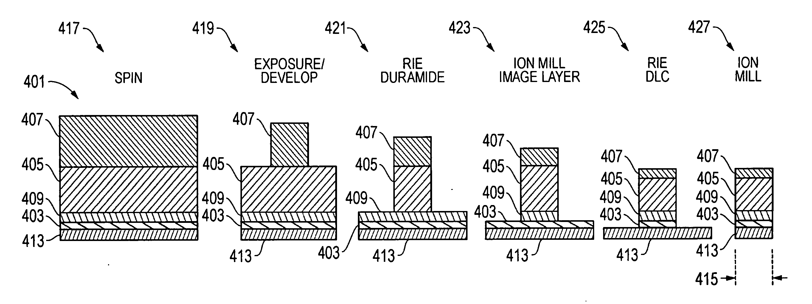
[0014] Referring to FIG. 3, one embodiment of the present invention is shown. At its most basic level, the present invention comprises a system and method of forming masks for structures having relatively narrow track widths. In this disclosure, “narrow” TWs are defined as those less than approximately 100 nm, but this depends upon the application and the processes used.

[0015] As shown in FIG. 3, one embodiment of the present invention comprises defining a structure 401 having a DLC layer 403, a duramide layer 405, and a TIS layer 407. At least one mask or image layer 409 of an RIE-resistant material is also provided. The image layer(s) 409 may be formed with ion milling, but other types of processes including, for example, RIE, ion milling, and reactive ion beam etching may be used as well. In addition, the image layer 409 may be formed from a variety of materials including, for example, Rh, Cu, NiFe, and the like, at a thickness of approximately 20 to 100 Å in one embodiment.

[00...


PUM


Abstract

A process for defining and controlling the track width for sensor devices is disclosed. An RIE-resistant, image layer, such as Cu or NiFe, is deposited after the DLC layer. A combination of RIE and ion milling processes or reactive ion beam etching processes are used to form the mask structure. Having an RIE-resistant layer precisely defines the DLC edge and minimizes the line edge roughness that result from fast removal of duramide during RIE. This solution controls the formation of the edges of the sensors and provides good definition for DLC mask edges. The image layer may be chemical mechanical polished to eliminate ion milling before the final RIE step.

Description

BACKGROUND OF THE INVENTION [0001] 1. Technical Field [0002] The present invention relates in general to the masking of devices during processing and, in particular, to an improved system and method for improved masking of sensors during processing for better sensor edge control and track width definition for sensors having a narrow track width. [0003] 2. Description of the Related Art [0004] Current mask processes can be prone to track width (TW) control and junction definition issues between the various layers of the product that define the sensor width. Some of these problems are illustrated in FIG. 1, which is a tunneling electron microscope (TEM) image of a sectioned masked wafer site 17. For example, the freelayer has a TW length 11 that is wider than the width 13 of the mask. In addition, the side 15 of the mask (e.g., into and out of the page) is relatively rough rather than straight, and the edges of the diamond-like carbon (DLC) mask layer are sloped rather than relatively...

Claims


Application Information

Patent Timeline
Patent Type & Authority Applications(United States)
IPC IPC(8): H01L21/00H01L21/302
CPCG11B5/3163G11B5/3116
Inventor PINARBASI, MUSTAFA MICHAEL
Owner WESTERN DIGITAL TECH INC
Why Eureka
Try Eureka