Novel phase change random access memory

Active Publication Date: 2007-01-18
TAIWAN SEMICON MFG CO LTD
View PDF13 Cites 83 Cited by
  • Summary
  • Abstract
  • Description
  • Claims
  • Application Information

AI Technical Summary

Benefits of technology

[0013] The preferred embodiments of the present invention have several advantageous features. Firstly, a single patterning and etching step is performed to form the bottom electrode portion and the (ARC) electrical insulating portion, thus reducing the complexity and cost of manufacturing processes. Sec

Problems solved by technology

The resistivity ratios of the phase change materials in the amorphous and crystalline states are typically greater than 1000 and thus the phase change memory devices are unlikely to have errors for reading states.
One engineering challenge in improving PRAM devices is to reduce the programming current required to effect

Method used


Image

  • Novel phase change random access memory
  • Novel phase change random access memory
  • Novel phase change random access memory

Examples


Embodiment Construction

[0018] The making and using of the presently preferred embodiments are discussed in detail below. It should be appreciated, however, that the present invention provides many applicable inventive concepts that can be embodied in a wide variety of specific contexts. The specific embodiments discussed are merely illustrative of specific ways to make and use the invention, and do not limit the scope of the invention.

[0019] The preferred embodiments are illustrated in FIGS. 3A through 8B, wherein like reference numbers are used to designate like elements throughout the various views and illustrative embodiments of the present invention. Throughout the description, each figure number may be followed by a letter A or B, indicating alternative steps or different views of forming the same structures.

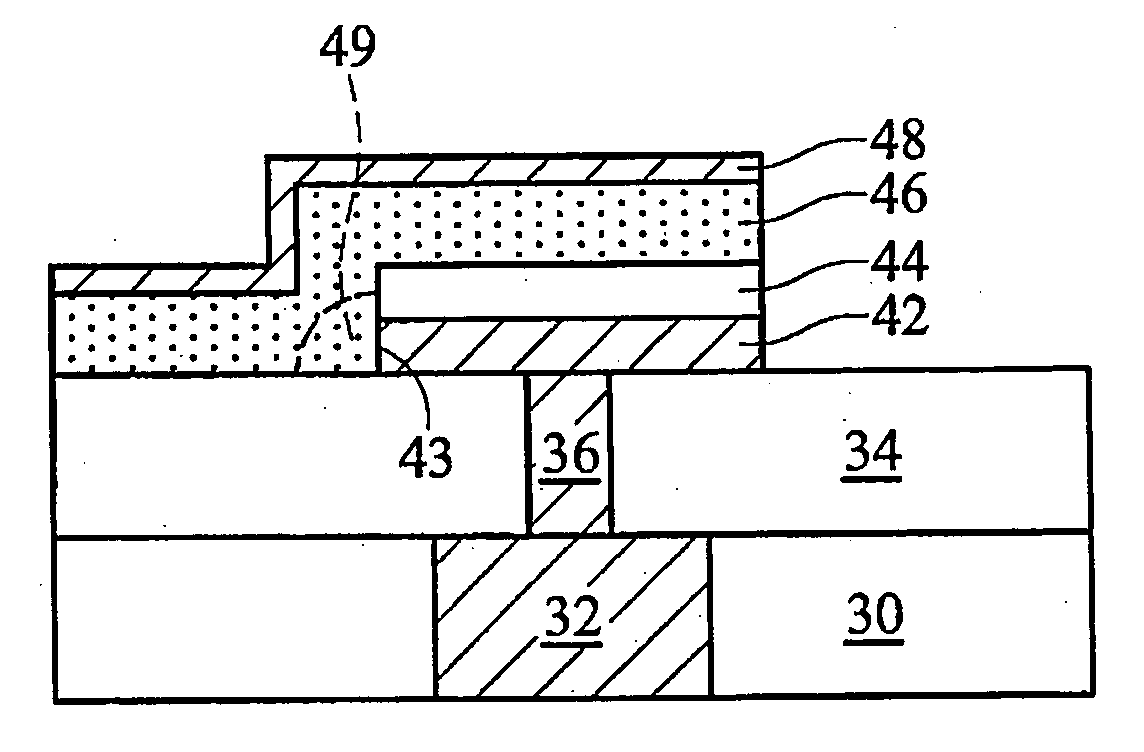
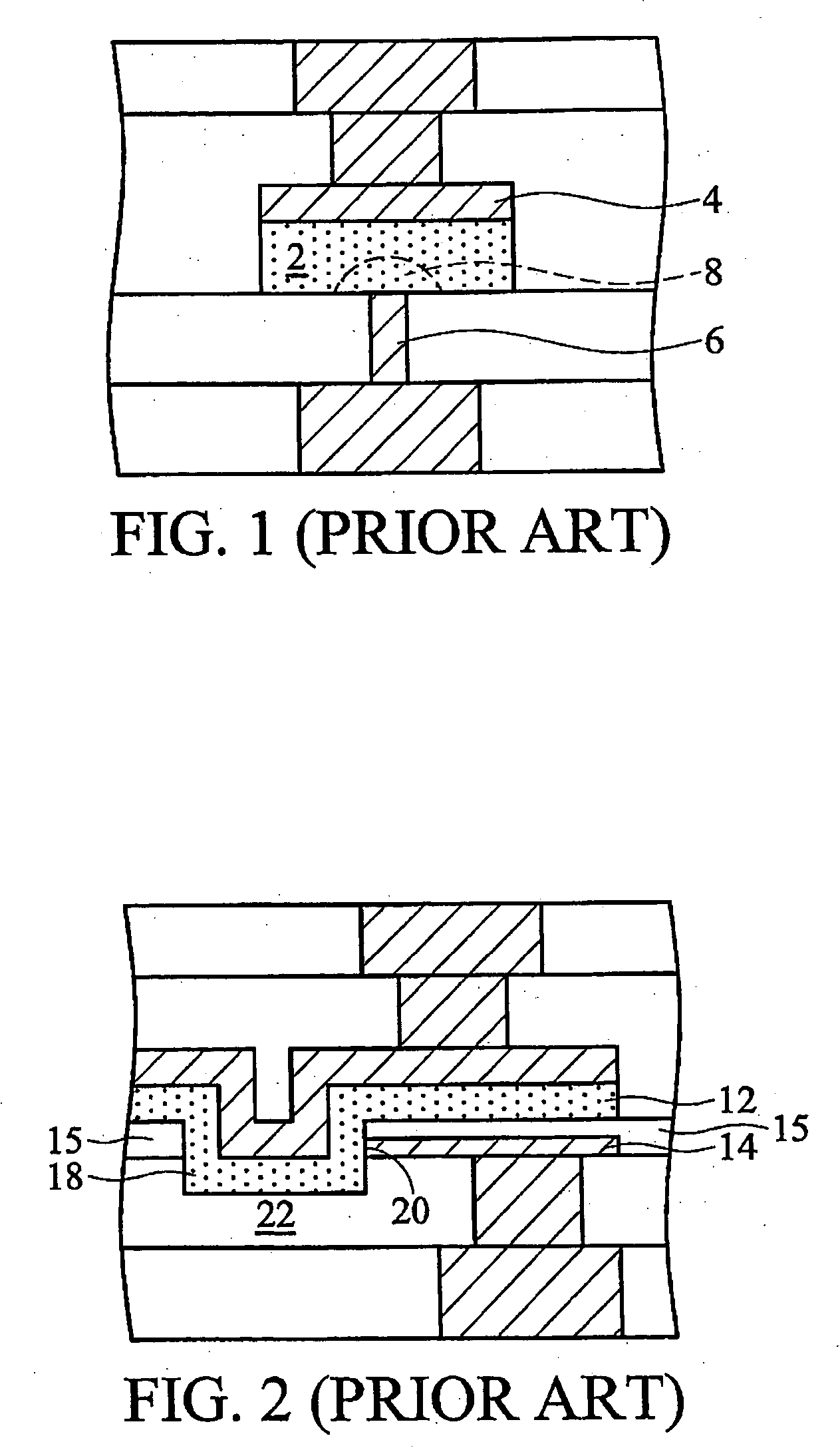
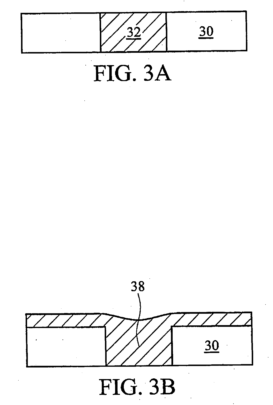
[0020] Referring to FIG. 3A, a conductive line 32 and an insulating layer 30 are formed in a first metallization layer. In one preferred embodiment, the conductive line 32 may be formed by a me...


PUM


Abstract

A phase change memory device with a reduced phase change volume and lower drive current and a method for forming the same are provided. The method includes forming a bottom insulating layer comprising a bottom electrode contact, forming a bottom electrode film on the bottom electrode contact, forming an anti-reflective coating (ARC) film on the bottom electrode film, patterning and etching the ARC film and the bottom electrode film to form a bottom electrode comprising a side edge, and forming a phase change material portion on the ARC film and the bottom insulating layer, wherein the phase change material portion physically contacts the side edge of the bottom electrode. The method further includes forming a top electrode on the phase change material portion, and forming a top electrode contact on the top electrode.

Description

[0001] This application relates to the following co-pending and commonly assigned patent application: application Ser. No. 10 / 783,498, filed Feb. 20, 2004, entitled “Phase Change Memory Cell and Method of Its Manufacture,” which application is incorporated herein by reference.TECHNICAL FIELD [0002] This invention generally relates to semiconductor devices and fabrication processes, and more particularly to a phase change random access memory device having a reduced phase change volume to improve device operation and a method of forming the same. BACKGROUND [0003] Phase change technology is promising for next generation memories. It uses chalcogenide semiconductors for storing states. The chalcogenide semiconductors, also called phase change materials, have a crystalline state and an amorphous state. In the crystalline state, the phase change materials have a low resistivity, while in the amorphous state they have a high resistivity. The resistivity ratios of the phase change materia...

Claims


Application Information

Patent Timeline
IPC IPC(8): H01L29/02
CPCH01L45/06H01L45/1233H01L45/122H01L45/144H01L45/126H10N70/821H10N70/8413H10N70/231H10N70/826H10N70/8828
Inventor HUANG, CHIEN-CHAO
Owner TAIWAN SEMICON MFG CO LTD
Why Eureka
Try Eureka