Substrate applicable to both wire bonding and flip chip bonding, smart card modules having the substrate and methods for fabricating the same

a smart card module and substrate technology, applied in the direction of printed circuit manufacturing, printed circuit aspects, instruments, etc., can solve the problems of difficult to perform wire bonding on a region of the substrate, high manufacturing cost of smart card modules according to conventional methods, etc., and achieve the effect of reducing the manufacturing cost of the substra

Inactive Publication Date: 2007-01-18
SAMSUNG ELECTRONICS CO LTD
View PDF6 Cites 11 Cited by
  • Summary
  • Abstract
  • Description
  • Claims
  • Application Information

AI Technical Summary

Benefits of technology

[0014] According to example embodiments of the present invention, the electrical connection between the upper metal layer and the bottom metal layer may be formed using a pressing process, a drilling process and / or a punching process without forming a micro via using the laser and so the manufacturing cost of the substrate may be reduced. A smart card module having the substrate in accordance with example embodiments of the present invention may be manufactured by wire bonding and / or flip chip bonding.

Problems solved by technology

Manufacturing the smart card module according to the conventional methods may be costly.
Also, it may be difficult to perform wire bonding on a region of the substrate where a via hole is activated.

Method used


Image

  • Substrate applicable to both wire bonding and flip chip bonding, smart card modules having the substrate and methods for fabricating the same
  • Substrate applicable to both wire bonding and flip chip bonding, smart card modules having the substrate and methods for fabricating the same
  • Substrate applicable to both wire bonding and flip chip bonding, smart card modules having the substrate and methods for fabricating the same

Examples


Embodiment Construction

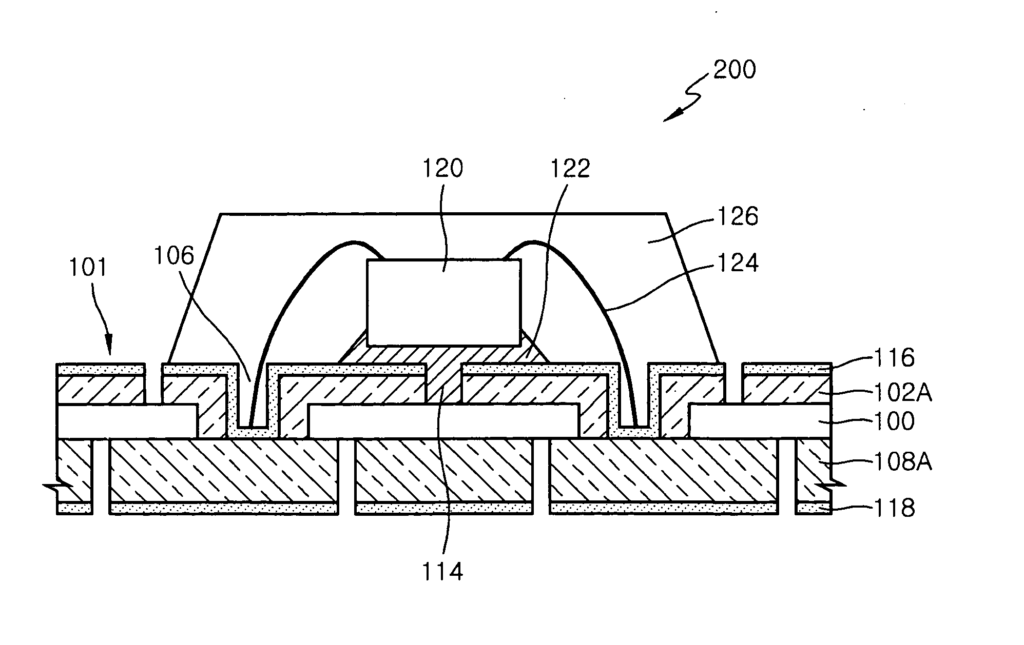
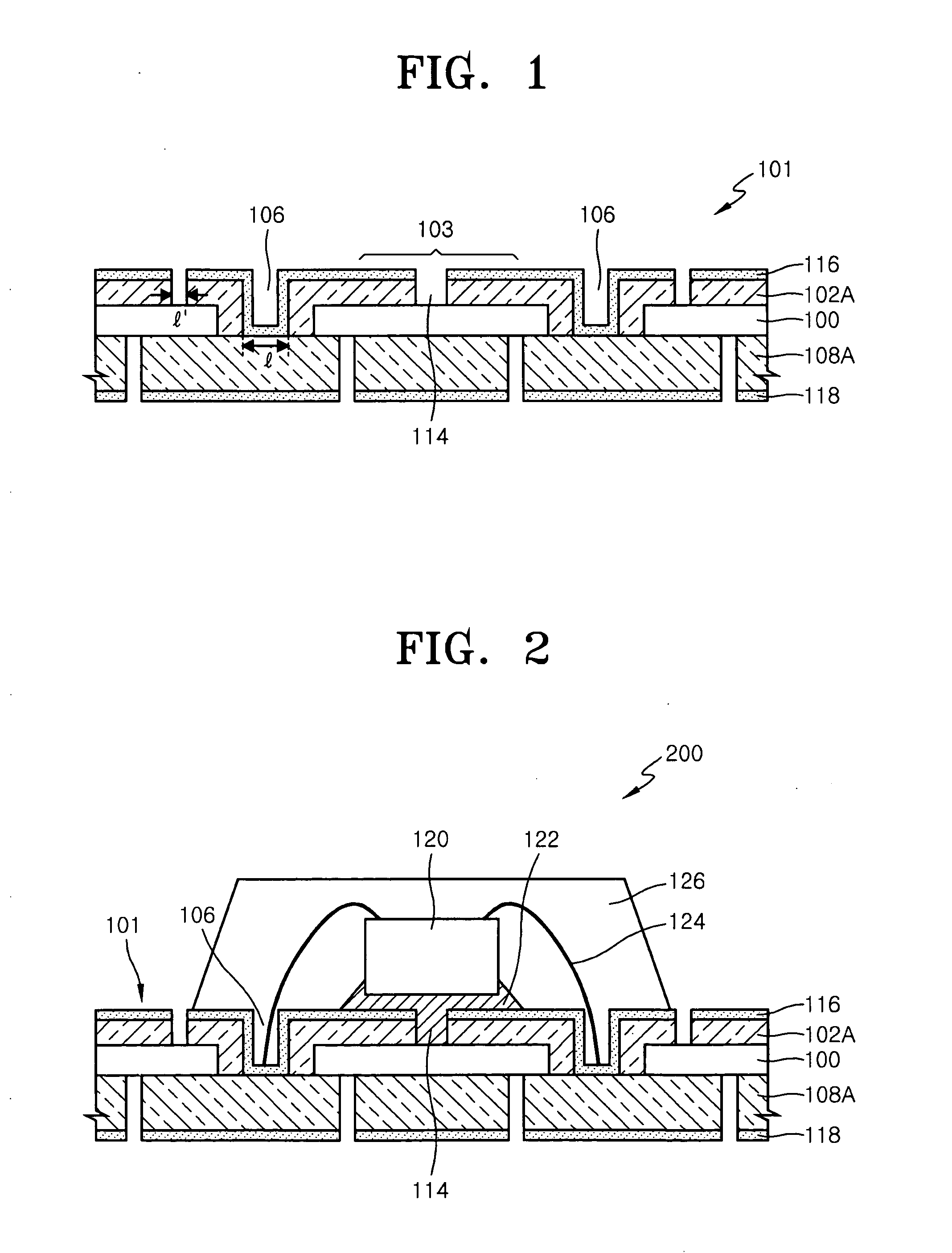
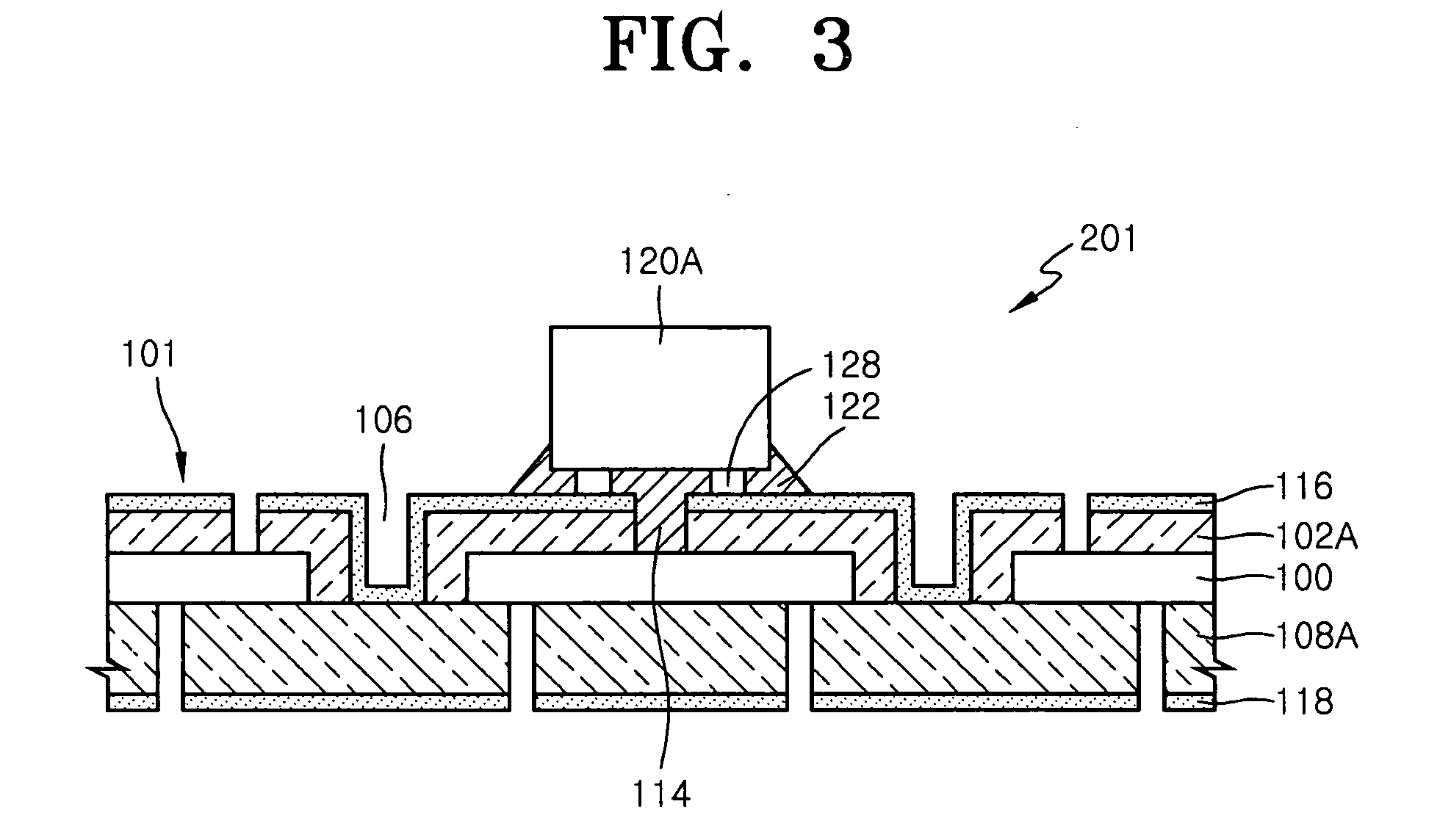
[0019] Various example embodiments of the present invention will now be described more fully with reference to the accompanying drawings, in which example embodiments of the present invention are shown. Example embodiments of the present invention should not be construed as being limited to the example embodiments set forth herein; rather, these example embodiments are provided so that this disclosure will be thorough and complete, and will fully convey the concept of the invention to those skilled in the art. Like numbers refer to like elements throughout the description of the figures.

[0020] Detailed illustrative embodiments of the present invention are disclosed herein. However, specific structural and functional details disclosed herein are merely representative for purposes of describing example embodiments of the present invention. This invention may, however, may be embodied in many alternate forms and should not be construed as limited to only the embodiments set forth here...


PUM

PropertyMeasurementUnit
thicknessaaaaaaaaaa
insulatingaaaaaaaaaa
sizeaaaaaaaaaa

Abstract

A substrate, a smart card module having the substrate and methods for fabricating the same are provided. A substrate having metal patterns formed on both sides and applicable to both wire bonding and flip chip bonding, a smart card module having the same and methods of fabricating the same are also provided. The substrate may include an insulating layer, an upper metal pattern, a bottom metal pattern, a first plating layer, a second plating layer and a substrate. The insulating layer may have a plurality of via holes. The upper metal pattern may be formed on the insulating layer and side surfaces of the plurality of via holes. The bottom metal pattern may be formed on the bottom of the insulating layer and electrically connected to the upper metal pattern. The first plating layer may be formed on the upper metal pattern and the upper surface of the bottom metal pattern. The second plating layer may be formed on the bottom of the bottom metal pattern. The substrate may include contact holes having side surfaces of the plurality of via holes covered by the upper metal pattern and the first plating layer. The bottom surface of the insulating layer may be supported by the bottom metal pattern and the first plating layer.

Description

PRIORITY STATEMENT [0001] This application claims priority under 35 U.S.C. § 119 to Korean Patent Application No. 10-2005-0064770, filed on Jul. 18, 2005, in the Korean Intellectual Property Office (KIPO), the entire contents of which are incorporated herein by reference. BACKGROUND [0002] 1. Field [0003] Example embodiments of the present invention relate to a substrate, a smart card module having the substrate and methods for fabricating the same. Other example embodiments of the present invention relate to a substrate having metal patterns formed on both sides and applicable to both wire bonding and flip chip bonding, a smart card module having the same and methods of fabricating the same. [0004] 2. Description of the Related Art [0005] The term “smart card” may be used in various industrial fields. In the international standardization organization (ISO), a smart card may be defined as a card including at least one of integrated circuits. In order to process given transactions, t...

Claims


Application Information

Patent Timeline
Patent Type & Authority Applications(United States)
IPC IPC(8): H01L21/76
CPCH01L21/563H01L2924/07802H01L23/49855H01L24/32H01L24/48H01L24/81H01L24/85H01L24/90H01L2221/68377H01L2224/05599H01L2224/16225H01L2224/32057H01L2224/32225H01L2224/48091H01L2224/48227H01L2224/48228H01L2224/484H01L2224/73204H01L2224/73265H01L2224/8121H01L2224/81815H01L2224/83102H01L2224/83192H01L2224/83385H01L2224/85399H01L2224/90H01L2224/92125H01L2924/01005H01L2924/01028H01L2924/01029H01L2924/01046H01L2924/01078H01L2924/01079H01L2924/01082H01L2924/014H01L2924/14H05K3/244H05K3/4084H05K2201/0394H05K2201/09472H05K2201/09509H05K2203/049H05K2203/1189H05K2203/1461H01L2924/00014H01L2924/01006H01L2924/01033H01L24/29H01L24/83H01L2224/0401H01L2924/15151H01L2224/26175H01L23/3121H01L2224/45099H01L2924/00012H01L2924/00H01L24/73H01L2924/181G06K19/07G06K19/077
Inventor LEE, SEOK-WONCHOI, KYOUNG-SEIKIM, DONG-HANRO, YOUNG-HOON
Owner SAMSUNG ELECTRONICS CO LTD
Why Eureka
Try Eureka