Vertical GaN-based LED and method of manfacturing the same

a technology of gan-based led and gan-based light, which is applied in the direction of semiconductor/solid-state device manufacturing, electrical equipment, semiconductor devices, etc., can solve the problems of poor thermal conductivity, limitation in reducing manufacturing costs, and rigid substrate of silicon substrate, etc., to achieve maximum improvement of external quantum efficiency, increase surface area, and high power characteristic

Active Publication Date: 2007-01-25
SAMSUNG ELECTRONICS CO LTD
View PDF4 Cites 146 Cited by
  • Summary
  • Abstract
  • Description
  • Claims
  • Application Information

AI Technical Summary

Benefits of technology

[0023] An advantage of the present invention is that it provides a vertical GaN-based LED that can maximize the improvement of an external quantum efficiency by forming uneven patterns as a macroscopic structure so as to increase a surface area and forming a plurality of protuberances, which are fine light-scattering structures, on a surface of the uneven patterns. Also, the vertical GaN-based LED can achieve a high power characteristic by improving the current dispersion effect.
[0024] Another advantage of the present invention is that it provides a method of manufacturing the vertical GaN-based LED.
[0025] Additional aspects and advantages of the present general inventive concept will be set forth in part in the description which follows and, in part, will be obvious from the description, or may be learned by practice of the general inventive concept.
[0026] According to an aspect of the invention, a vertical GaN-based LED includes an n-electrode; a first n-type GaN layer having uneven patterns having a plurality of protuberances for increasing a surface area and formed under the n-electrode; a first AlGaN layer formed under the first n-type GaN layer; a GaN layer formed under the first AlGaN layer; a second AlGaN layer formed under the GaN layer; a second n-type GaN layer formed under the second AlGaN layer; an active layer formed under the second n-type GaN layer; a p-type GaN layer formed under the active layer; a p-electrode formed under the p-type GaN layer; and a structure support layer formed under the p-electrode.
[0027] Each of the uneven patterns has a lower width of 0.5 μm to 5 μm and has a height of 0.1 μm to 5 μm.
[0028] Each of the uneven patterns has a lateral side tapered upwardly, and preferably, has a hemispherical pattern arranged vertically and horizontally.

Problems solved by technology

Generally, a GaN-based LED is grown on a sapphire substrate, but the sapphire substrate is a rigid nonconductor and has poor thermal conductivity.
Therefore, there is a limitation in reducing the manufacturing costs by decreasing the size of a GaN-based LED, or improving the optical power and chip characteristic.
However, the conventional vertical GaN-based LED has a problem in that photon generated from an active layer is emitted to the outside of the LED.
However, according to the vertical GaN-based LED manufactured by the method disclosed in U.S. Patent Publication No. 20030222263, when the LED structure 16 has a thickness of 10 μm or less (thin GaN), the process of forming the photoresist patterns 32 and subsequent processes are difficult to carry out even if the silicon substrate acting as a sub support is used.
In addition, because the patterns for improving the external quantum efficiency are formed in a convex hemispherical shape on the surface of the LED structure, the surface of the LED structure on which the patterns can be formed is limited.
Accordingly, the improvement of the external quantum efficiency that can be obtained by applying the convex hemispherical patterns is not sufficient.
Consequently, the light-extraction efficiency of the LED is degraded and the lifespan of the LED is reduced.

Method used


Image

  • Vertical GaN-based LED and method of manfacturing the same
  • Vertical GaN-based LED and method of manfacturing the same
  • Vertical GaN-based LED and method of manfacturing the same

Examples


Embodiment Construction

[0051] Reference will now be made in detail to the embodiments of the present general inventive concept, examples of which are illustrated in the accompanying drawings, wherein like reference numerals refer to the like elements throughout. The embodiments are described below in order to explain the present general inventive concept by referring to the figures.

[0052] Hereinafter, a vertical GaN-based LED and a method of manufacturing the same according to the embodiments of the present invention will be described in detail with reference to the accompanying drawings.

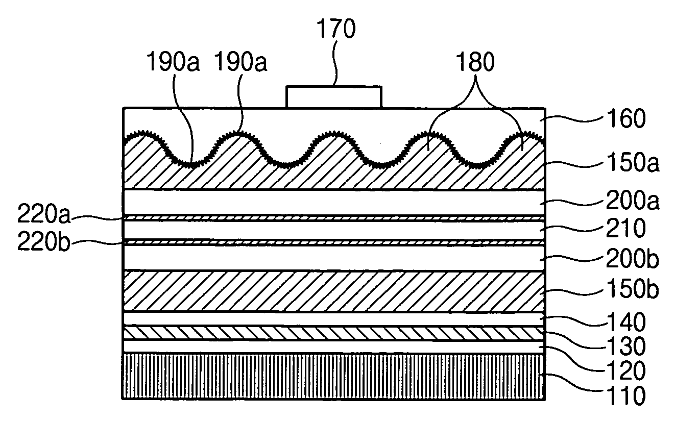
[0053] [Structure of Vertical GaN-Based LED]

[0054] A structure of a vertical GaN-based LED according to an embodiment of the present invention will be described in detail with reference to FIGS. 5 to 7B.

[0055]FIG. 5 is a perspective view of a vertical GaN-based LED according to an embodiment of the present invention, FIG. 6 is a schematic view of uneven patterns in the vertical GaN-based LED of FIG. 5, and FIGS. 7A and...


PUM


Abstract

A vertical GaN-based LED and a method of manufacturing the same are provided. The vertical GaN-based LED includes an n-electrode, a first n-type GaN layer, a first AlGaN layer, a GaN layer, a second AlGaN layer, a second n-type GaN layer, an active layer, a p-type GaN layer, and a structure support layer. The first n-type GaN layer has uneven patterns having a plurality of protuberances. The first AlGaN layer is formed under the first n-type GaN layer, and the GaN layer is formed under the first AlGaN layer. The active layer is formed under the second n-type GaN layer, and the p-type GaN layer is formed under the active layer. A p-electrode is formed under the p-type GaN layer, and the structure support layer is formed under the p-electrode.

Description

CROSS-REFERENCE TO RELATED APPLICATIONS [0001] This application claims the benefit of Korean Patent Application No. 2005-0066621 filed with the Korea Intellectual Property Office on Jul. 22, 2005, the disclosure of which is incorporated herein by reference. BACKGROUND OF THE INVENTION [0002] 1. Field of the Invention [0003] The present invention relates to a vertical (vertical-electrode-type) GaN-based light emitting diode (LED) and a method of manufacturing the same, and more particularly, to a vertical GaN-based LED and a method of manufacturing the same, capable of increasing the external quantum efficiency and the manufacturing yield by optimizing the current diffusion effect and increasing the light-extraction efficiency. [0004] 2. Description of the Related Art [0005] Generally, a GaN-based LED is grown on a sapphire substrate, but the sapphire substrate is a rigid nonconductor and has poor thermal conductivity. Therefore, there is a limitation in reducing the manufacturing co...

Claims


Application Information

Patent Timeline
Patent Type & Authority Applications(United States)
IPC IPC(8): H01L33/00H01L21/00H01L33/06H01L33/12H01L33/22H01L33/32
CPCH01L33/22H01L33/14
Inventor LEE, JAE HOONOH, BANG WONCHOI, HEE SEOKOH, JEONG TAKCHOI, SEOK BEOMLEE, SU YEOL
Owner SAMSUNG ELECTRONICS CO LTD
Why Eureka
Try Eureka