Electron emission device, electron emission type backlight unit and flat display apparatus having the same

a technology of electron emission and backlighting, which is applied in the direction of discharge tube/lamp details, discharge tube luminescnet screens, discharge tube main electrodes, etc., can solve the problems of affecting the energy efficiency of electron emission by a high anode voltage, the inability of other incident electrons to contribute to light emission, and the inability to improve light-emitting efficiency. , to achieve the effect of improving light-emitting efficiency, improving electron emission efficiency, and improving light-emitting efficiency ratio

Inactive Publication Date: 2007-01-25
SAMSUNG SDI CO LTD
View PDF33 Cites 8 Cited by
  • Summary
  • Abstract
  • Description
  • Claims
  • Application Information

AI Technical Summary

Benefits of technology

[0016] Aspects of the present invention provide an electron emission device with improved electron emission efficiency and an electron emission type backlight unit with a new structure using the electron emission device in which an electric field between an anode electrode and a cathode electrode is effectively blocked, and electrons are emitted continuously and stably by a low gate voltage thereby improving light-emitting uniformity and light-emitting efficiency.

Problems solved by technology

In addition, due to the light-emitting characteristic of phosphor materials, during a predetermined period of time in which light is being emitted by electrons that are incident on the phosphor materials, other incident electrons cannot contribute to light emitting.
Thus, light-emitting efficiency is not improved by increasing incident electrons beyond this saturation level on the phosphor layer 70 and electron emission by a high anode voltage is detrimental from an energy efficiency aspect.
However, when electrons are emitted by a strong anode voltage, efficient electron emission and light emitting become impossible.

Method used


Image

  • Electron emission device, electron emission type backlight unit and flat display apparatus having the same
  • Electron emission device, electron emission type backlight unit and flat display apparatus having the same
  • Electron emission device, electron emission type backlight unit and flat display apparatus having the same

Examples


Embodiment Construction

[0043] Reference will now be made in detail to the present embodiments of the present invention, examples of which are illustrated in the accompanying drawings, wherein like reference numerals refer to the like elements throughout. The embodiments are described below in order to explain the present invention by referring to the figures.

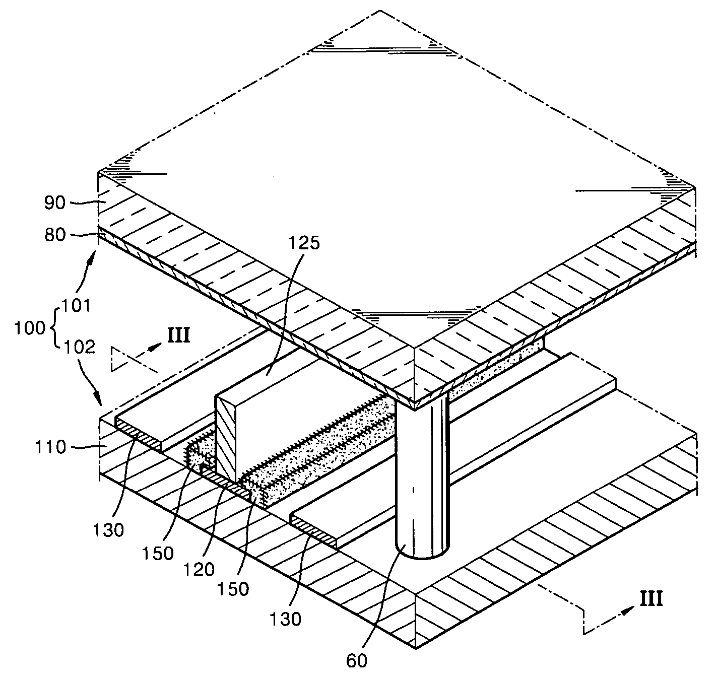
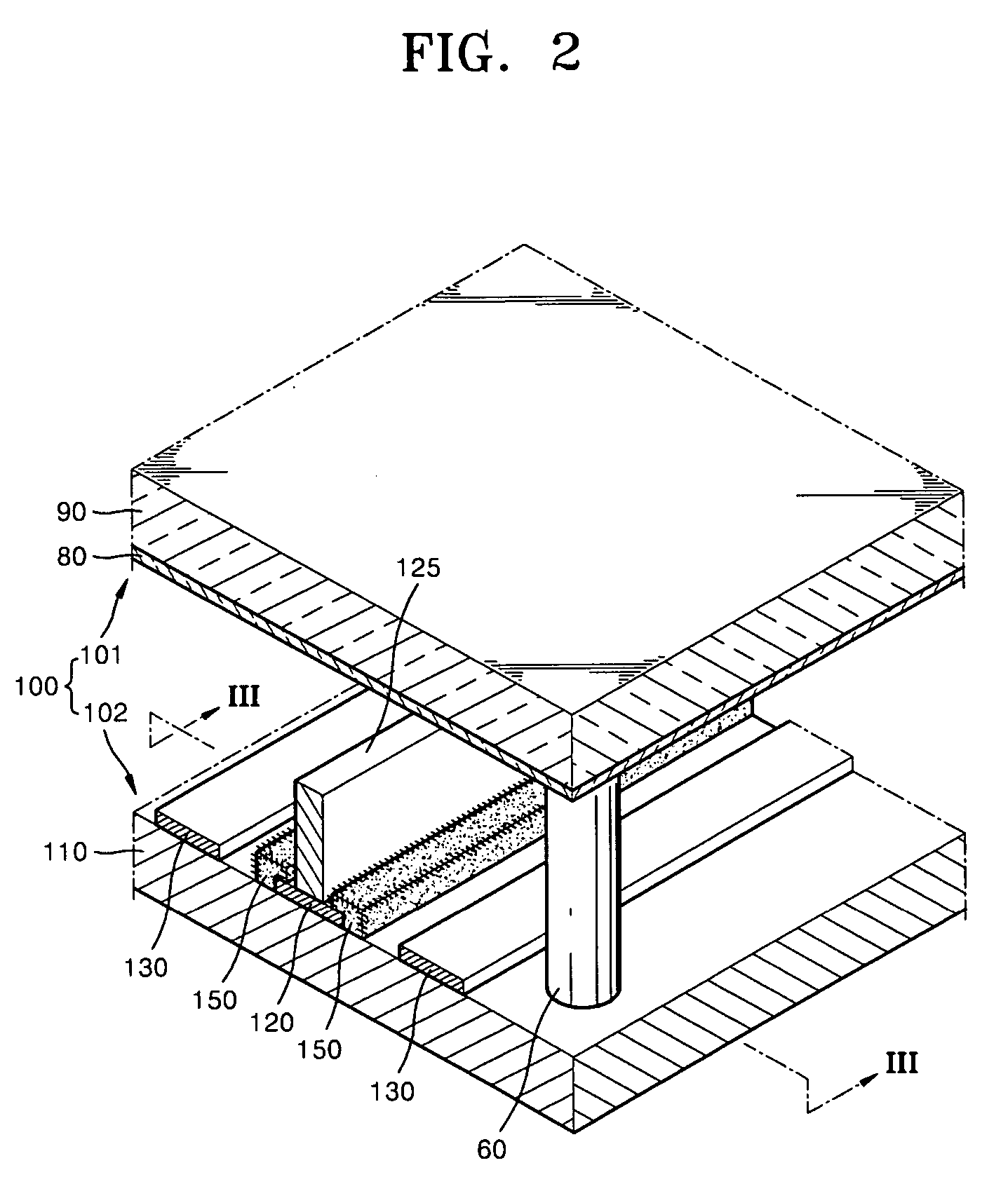
[0044]FIG. 2 is a perspective view of an electron emission type backlight unit 100 according to an embodiment of the present invention; FIG. 3 is a cross-sectional view of the electron emission type backlight unit 100 of FIG. 2 cut along a line III-III.

[0045] Referring to FIGS. 2 and 3, the electron emission type backlight unit 100 includes a front panel 101 and an electron emission device 102 that face each other and are disposed parallel to each other to form a vacuum space 103, and a spacer 60 which maintains a distance between the front panel 101 and the electron emission device 102.

[0046] The front panel 101 includes a front substrate 90, an a...


PUM


Abstract

An electron emission device with improved electron emission efficiency and an electron emission type backlight unit with a new structure using the electron emission device in which an electric field between an anode electrode and a cathode electrode is effectively blocked, and electrons are emitted continuously and stably by a low gate voltage thereby improving light-emitting uniformity and light-emitting efficiency. Also provided is a flat display apparatus employing the electron emission type backlight unit having the electron emission device. The electron emission device includes a base substrate; a cathode electrode formed on the base substrate; a gate electrode that is formed on the base substrate and alternately separated from the cathode electrode when there are more than one; an electron emission layer disposed on a surface of the cathode electrode; and a supplementary electrode formed on the cathode electrode or the gate electrode and is higher than the corresponding electrode.

Description

CROSS-REFERENCE TO RELATED APPLICATIONS [0001] This application claims the benefit of Korean Application No. 2005-65428, filed Jul. 29, 2005, in the Korean Intellectual Property Office, the disclosure of which is incorporated herein in its entirety by reference. BACKGROUND OF THE INVENTION [0002] 1. Field of the Invention [0003] Aspects of the present invention relate to an electron emission device, an electron emission type backlight unit, and a flat display apparatus having the same, and more particularly, to an electron emission device with improved electron emission efficiency and light-emitting uniformity, an electron emission type backlight unit employing the electron emission device, and a flat display apparatus having the electron emission type backlight unit. [0004] 2. Description of the Related Art [0005] Generally electron emission devices can be classified into electron emission devices using a thermionic cathode and electron emission devices using a cold cathode as an e...

Claims


Application Information

Patent Timeline
Patent Type & Authority Applications(United States)
IPC IPC(8): H01J1/62
CPCH01J3/021H01J3/08H01J63/06H01J31/127H01J63/02H01J29/481H01J1/30
Inventor CHO, YOUNG-SUKBAE, JAE-WOOLIM, IK-CHULCHOI, YONG-SOO
Owner SAMSUNG SDI CO LTD
Why Eureka
Try Eureka