Plasma display panel and flat lamp using boron nitride bamboo shoot

Inactive Publication Date: 2006-03-16
SAMSUNG SDI CO LTD
View PDF3 Cites 7 Cited by
  • Summary
  • Abstract
  • Description
  • Claims
  • Application Information

AI Technical Summary

Benefits of technology

[0009] The present invention provides a plasma display panel (PDP) and a flat lamp having improved durabilit

Problems solved by technology

However, the MgO protective layer has a limited ability to emit secondary electrons into the discharge space.
However, the CNT 22 ma

Method used


Image

  • Plasma display panel and flat lamp using boron nitride bamboo shoot
  • Plasma display panel and flat lamp using boron nitride bamboo shoot
  • Plasma display panel and flat lamp using boron nitride bamboo shoot

Examples


second embodiment

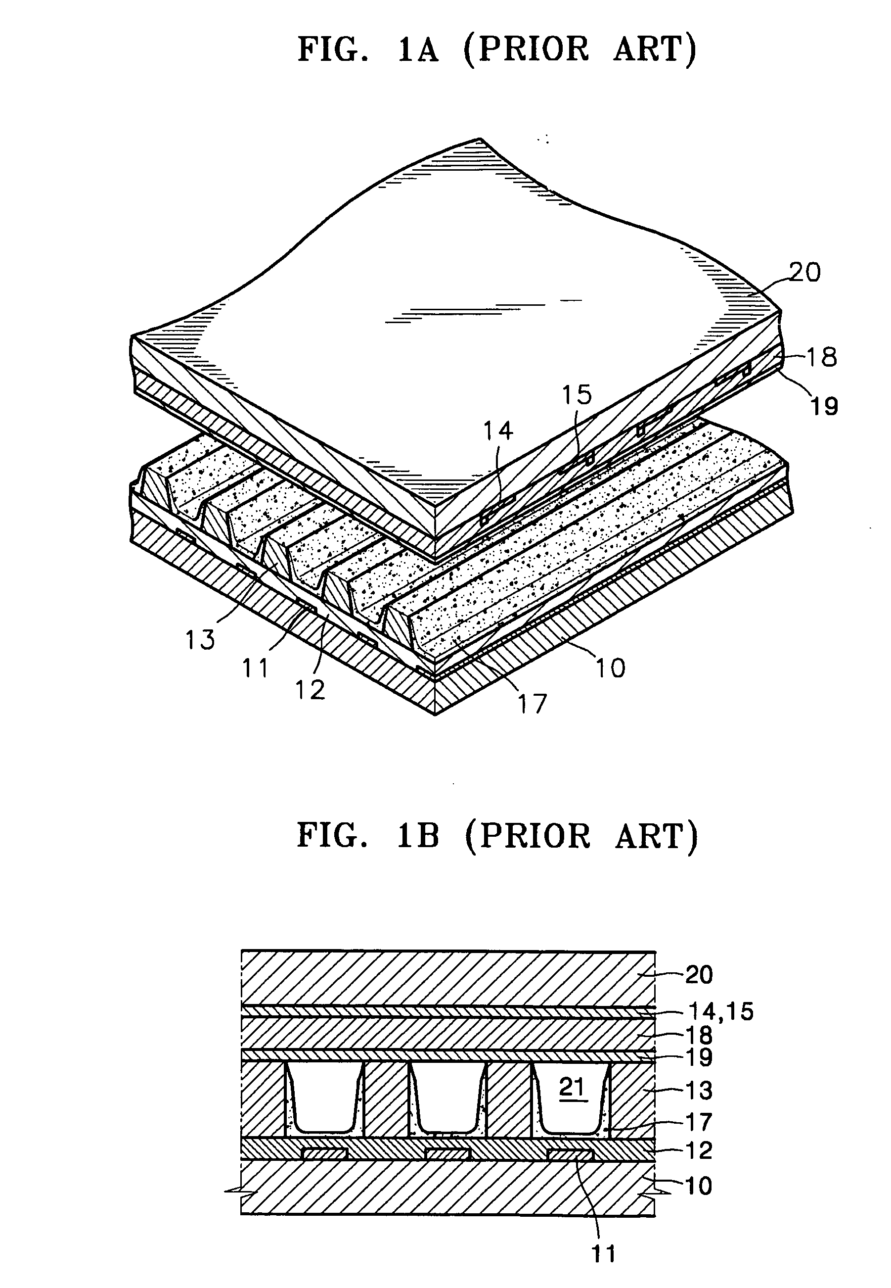
[0042]FIG. 10A and FIG. 10B are views showing modified examples of the PDP according to FIG. 9. In FIG. 10A, the MgO protective layer 46 is applied on an upper surface of the dielectric layer 43 and an upper surface of the secondary electron emission electrode 44. As described above, the MgO protective layer 46 prevents the dielectric layer 43 from being physically and chemically damaged, and it emits secondary electrons. Additionally, since the secondary electron emission electrode 44 comprising the BNBS layer 44b is durable and efficient, the MgO protective layer 46 may be formed only on the dielectric layer 43, as FIG. 10B shows. In this case, the dielectric layer 43 is formed slightly lower than the sum of the heights of the sustain electrode 41 and the secondary electron emission electrode 44. Additionally, a thin MgO protective layer 46 is formed on the upper surface of the dielectric layer 43 but not on the secondary electron emission electrode 44. Thus, the secondary electro...

third embodiment

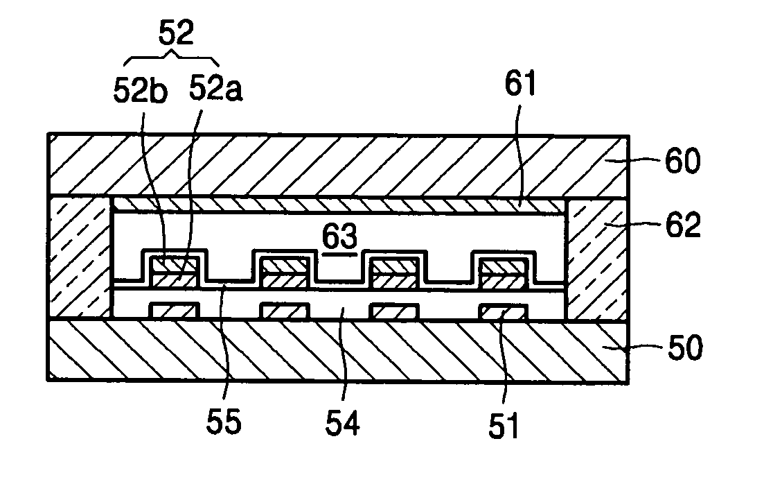
[0045] In the above embodiments, the secondary electron emission electrode is formed on the sustain electrode of the front substrate, however, the secondary electron emission electrode may also be formed on an address electrode of a rear substrate. FIG. 13 is a cross-sectional view showing a rear substrate of a PDP, in which the secondary electron emission electrode is formed on the address electrode, according to a third exemplary embodiment of the present invention. As FIG. 13 shows, the rear substrate unit of the PDP according to the present invention includes a rear substrate 30 that is formed of a transparent material such as a glass, a plurality of address electrodes 31 formed on the rear substrate 30 in parallel to each other, a secondary electron emission electrode 32 formed on the address electrode 31, a dielectric layer 33 covering the address electrodes 31 and the secondary electron emission electrodes 32, a plurality of barrier ribs 34 disposed on the dielectric layer 33...


PUM


Abstract

A plasma display panel (PDP) and a flat lamp using a boron nitride bamboo shoot (BNBS). The PDP includes a front substrate and a rear substrate opposing each other and having a plurality of discharge cells between them, a plurality of address electrodes arranged on the rear substrate in parallel to each other, a plurality of sustain electrodes arranged on the front substrate in parallel to each other and crossing the address electrodes, a dielectric layer arranged on the sustain electrodes, and a plurality of secondary electron emission electrodes arranged on the dielectric layer in parallel to each other and corresponding to the sustain electrodes, respectively. The secondary electron emission electrodes include the BNBS.

Description

CROSS REFERENCE TO RELATED APPLICATION [0001] This application claims priority to and the benefit of Korean Patent Application No. 10-2004-0073085, filed on Sep. 13, 2004, which is hereby incorporated by reference for all purposes as if fully set forth herein. BACKGROUND OF THE INVENTION [0002] 1. Field of the Invention [0003] The present invention relates to a plasma display panel and a flat lamp, and more particularly, to a plasma display panel and a flat lamp using a boron nitride bamboo shoot (BNBS). [0004] 2. Discussion of the Background [0005]FIG. 1A is a perspective view showing a general three-electrode surface discharge plasma display panel (PDP), and FIG. 1B and FIG. 1C are cross-sectional views showing the PDP of FIG. 1A cut in a width direction and a length direction, respectively. As shown in FIG. 1A, FIG. 1B and FIG. 1C, the PDP includes a front glass substrate 20 and a rear glass substrate 10 facing each other with a predetermined gap therebetween, barrier ribs 13 div...

Claims


Application Information

Patent Timeline
IPC IPC(8): H01J17/49H01J11/22H01J11/24H01J11/34H01J11/40H01J61/06H01J61/30H01J65/00
CPCH01J11/12H01J11/28H01J61/547H01J61/305H01J61/545H01J61/04H01J11/22H01J11/24
Inventor HATANAKA, HIDEKAZUKIM, YOUNG-MOLOO, HO-NYEONSON, SEUNG-HYUNJANG, SANG-HUNLEE, SEONG-EUIKIM, GI-YOUNGPARK, HYOUNG-BIN
Owner SAMSUNG SDI CO LTD
Why Eureka
Try Eureka