Composition for forming electron emission sources, method of manufacturing the same, and electron emission sources and electron emission device manufactured using the method

a technology of emission source and emission source, which is applied in the manufacture of electrode systems, electric discharge tubes/lamps, and discharge tubes luminescent screens, etc., can solve the problems of screen effect, ineffective use of electron emitters, and inability to uniformly emit electrons, so as to improve electron emission efficiency and improve electron emission efficiency

Inactive Publication Date: 2008-07-24
SAMSUNG SDI CO LTD
View PDF5 Cites 7 Cited by
  • Summary
  • Abstract
  • Description
  • Claims
  • Application Information

AI Technical Summary

Benefits of technology

[0015]It is therefore a feature of an embodiment of the present invention to provide electron emission sources that may prevent a screen effect and improve electron emission efficiency, and an electron emission device, a method of manufacturing the electron emission device, and a composition for forming the electron emission sources.
[0016]It is therefore another feature of an embodiment of the present invention to provide electron emission sources that may have improved electron emission efficiency by uniformly disposing electron emission materials on a surface of the electron emission sources, and an electron emission device, a method of manufacturing the electron emission device, and a composition for forming the electron emission sources.

Problems solved by technology

Therefore, the electron emitter may not be effectively used.
Therefore, electrons may not be uniformly emitted.
When end portions of electron emission materials are not spaced apart from each other by a predetermined gap, the closely packed electron emission materials may interact with an electron emission material having a large diameter, which may cause a screen effect such that electron emission characteristics deteriorate due to a large slenderness ratio.
Therefore, since the electron emission characteristics may deteriorate and a screen may not be uniform, a technology is desired to reduce or eliminate the above problems.

Method used


Image

  • Composition for forming electron emission sources, method of manufacturing the same, and electron emission sources and electron emission device manufactured using the method
  • Composition for forming electron emission sources, method of manufacturing the same, and electron emission sources and electron emission device manufactured using the method
  • Composition for forming electron emission sources, method of manufacturing the same, and electron emission sources and electron emission device manufactured using the method

Examples


Embodiment Construction

[0029]Korean Patent Application No. 10-2006-0038858, filed on Apr. 28, 2006, in the Korean Intellectual Property Office, and entitled: “Composition for Forming Electron Emission Sources, Method Of Manufacturing the Same, and Electron Emission Sources and Electron Emission Device Manufactured Using the Method,” is incorporated by reference herein in its entirety.

[0030]The present invention will now be described more fully hereinafter with reference to the accompanying drawings, in which exemplary embodiments of the invention are illustrated. The invention may, however, be embodied in different forms and should not be construed as limited to the embodiments set forth herein. Rather, these embodiments are provided so that this disclosure will be thorough and complete, and will fully convey the scope of the invention to those skilled in the art.

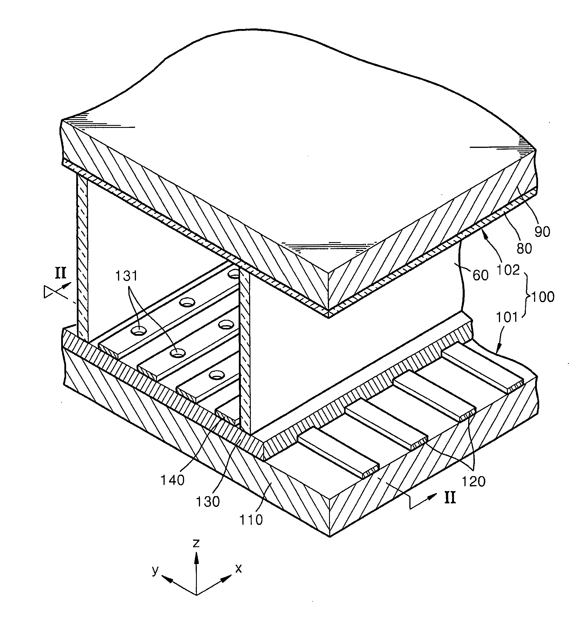
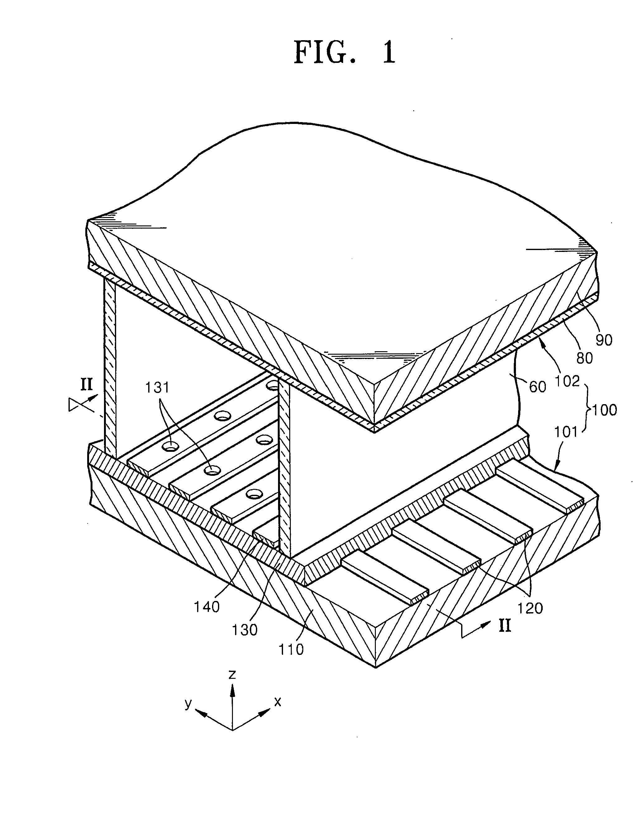
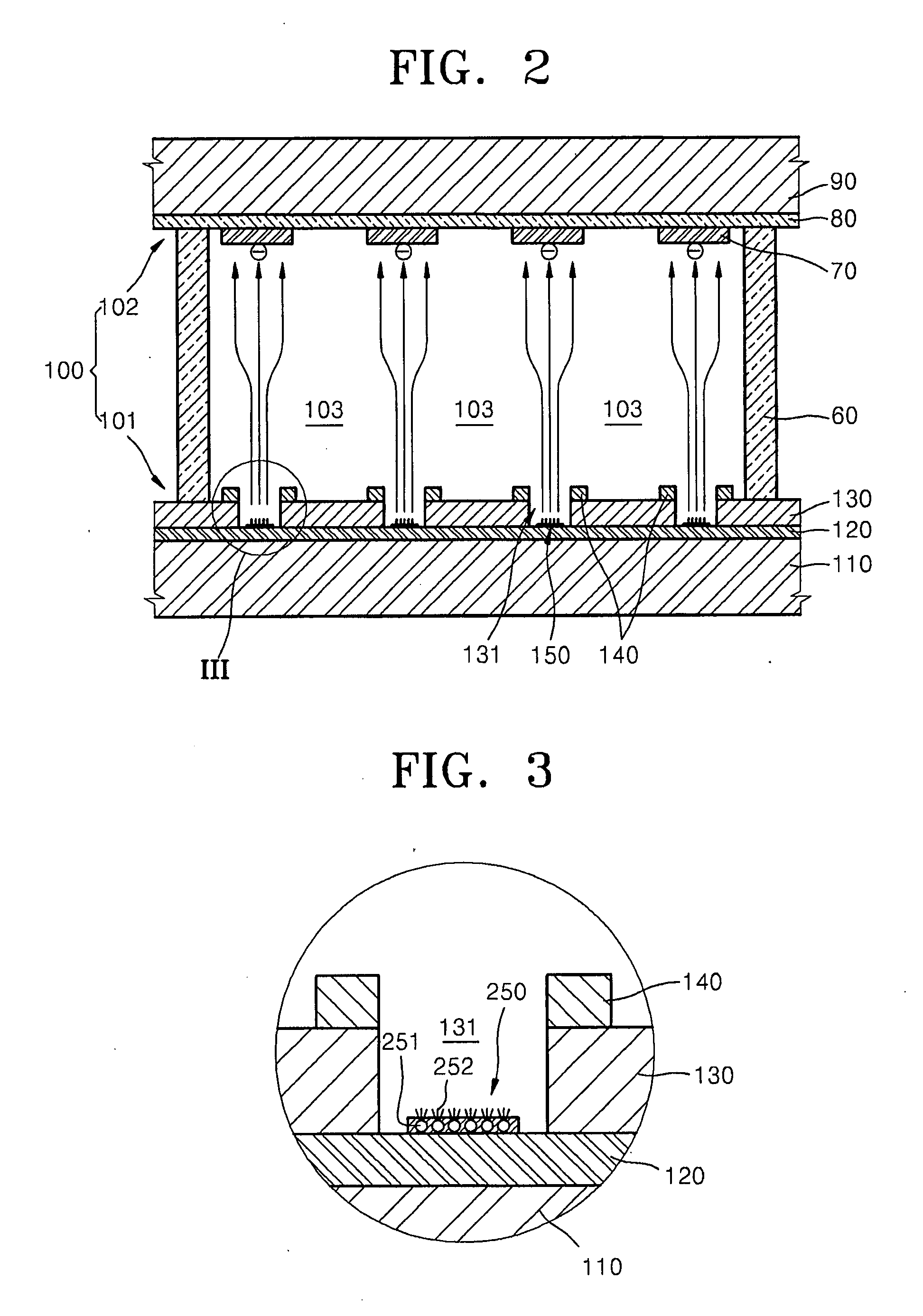
[0031]In the drawing figures, the dimensions of layers and regions may be exaggerated for clarity of illustration. It will also be understood th...


PUM


Abstract

An electron emission device includes a base substrate, first electrodes on the base substrate, second electrodes electrically insulated from the first electrodes, a first insulation layer between the first electrodes and the second electrodes, electron emission source holes formed in the first insulation layer and the second electrodes to expose the first electrodes, and electron emission sources in the electron emission source holes, each electron emission source including at least one electron emission material and at least one catalyst metal nano particle.

Description

BACKGROUND OF THE INVENTION[0001]1. Field of the Invention[0002]The present invention relates to a composition for forming electron emission sources, a method of manufacturing the same, electron emission sources and an electron emission device manufactured using the method. More particularly, the present invention relates to electron emission sources having improved electron emission efficiency by uniformly disposing electron emission materials on a surface of the electron emission sources, an electron emission device formed from the electron emission sources, a method of manufacturing the electron emission device, and a composition for forming the electron emission sources.[0003]2. Description of the Related Art[0004]In general, electron emission devices use a thermal cathode or a cold cathode as an electron emission source. Electron emission devices that use the cold cathode include, e.g., field emission device (FED) type electron emission devices, surface conduction emitter (SCE)...

Claims


Application Information

Patent Timeline
Patent Type & Authority Applications(United States)
IPC IPC(8): H01J1/62
CPCH01J1/304H01J1/3048H01J29/04H01J2329/0455H01J2201/30453H01J2201/30469H01J2329/0444H01J31/127B82Y40/00H01J9/02
Inventor JEONG, KWANG-SEOK
Owner SAMSUNG SDI CO LTD
Why Eureka
Try Eureka