Electronic device, method of driving the same, electro-optical device, and electronic apparatus

a technology of electro-optical devices and electronic devices, applied in the direction of instruments, static indicating devices, etc., can solve the problems of reducing the aperture ratio, and complicated configuration of the unit circui

Inactive Publication Date: 2007-01-25
SEIKO EPSON CORP
View PDF13 Cites 44 Cited by
  • Summary
  • Abstract
  • Description
  • Claims
  • Application Information

AI Technical Summary

Benefits of technology

[0007] An advantage of some aspects of the invention is that it realizes initialization of a gate of a driving transistor, without complicating the configuration of each unit circuit
[0008] Another advantage of some aspects of the invention is that it controls a driving period of a driven element, without complicating the configuration of each unit circuit.

Problems solved by technology

However, according to this configuration, due to the addition of the wiring lines or switching elements, the configuration of each unit circuit is complicated, and an aperture ratio is decreased.
Accordingly, there is problem in that the configuration of the unit circuit is complicated, or an aperture ratio is decreased.

Method used


Image

  • Electronic device, method of driving the same, electro-optical device, and electronic apparatus
  • Electronic device, method of driving the same, electro-optical device, and electronic apparatus
  • Electronic device, method of driving the same, electro-optical device, and electronic apparatus

Examples


first embodiment

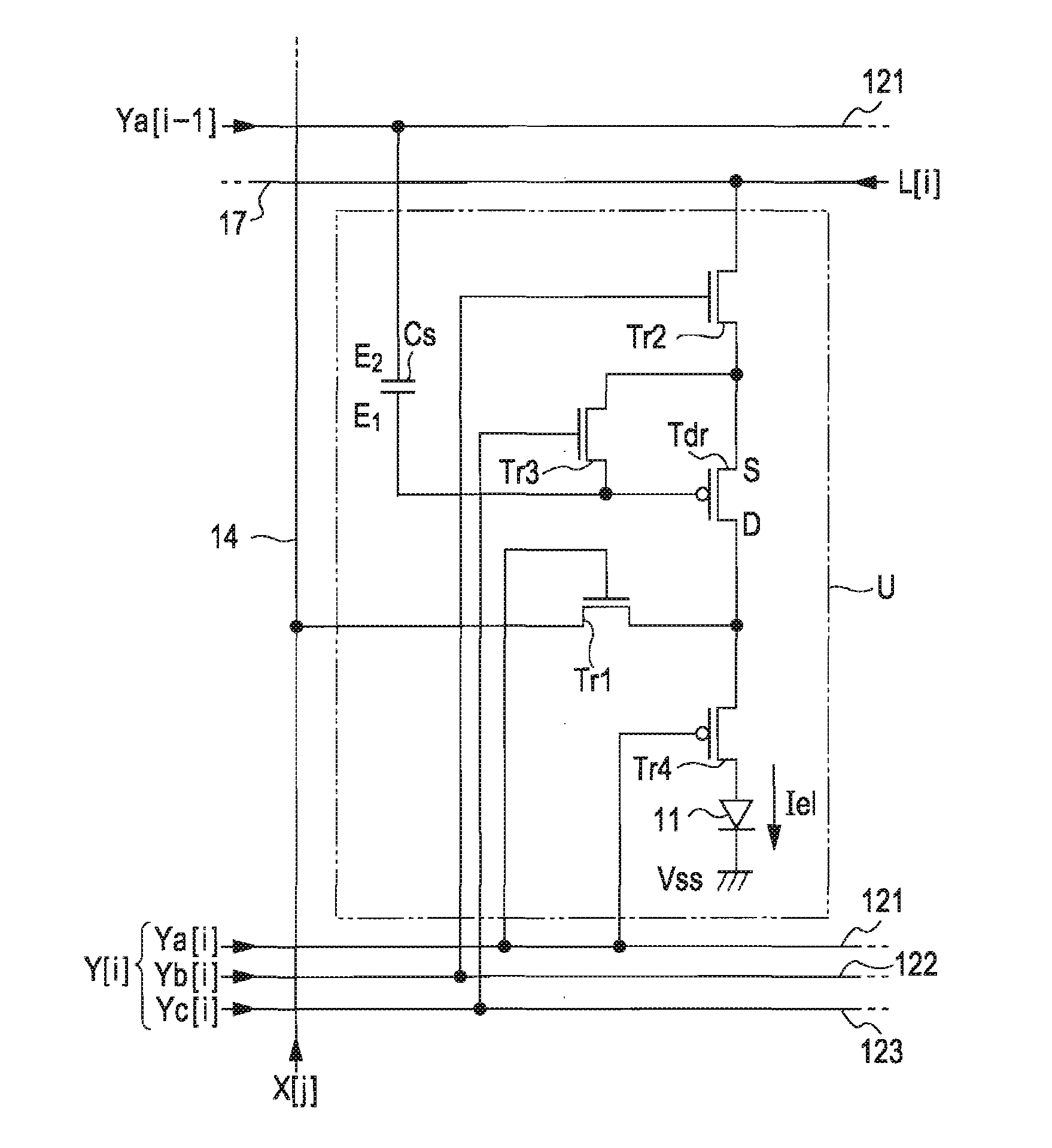
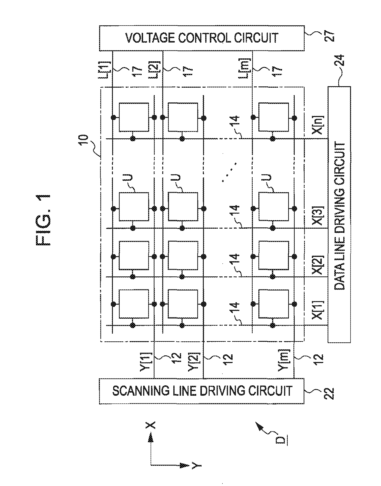
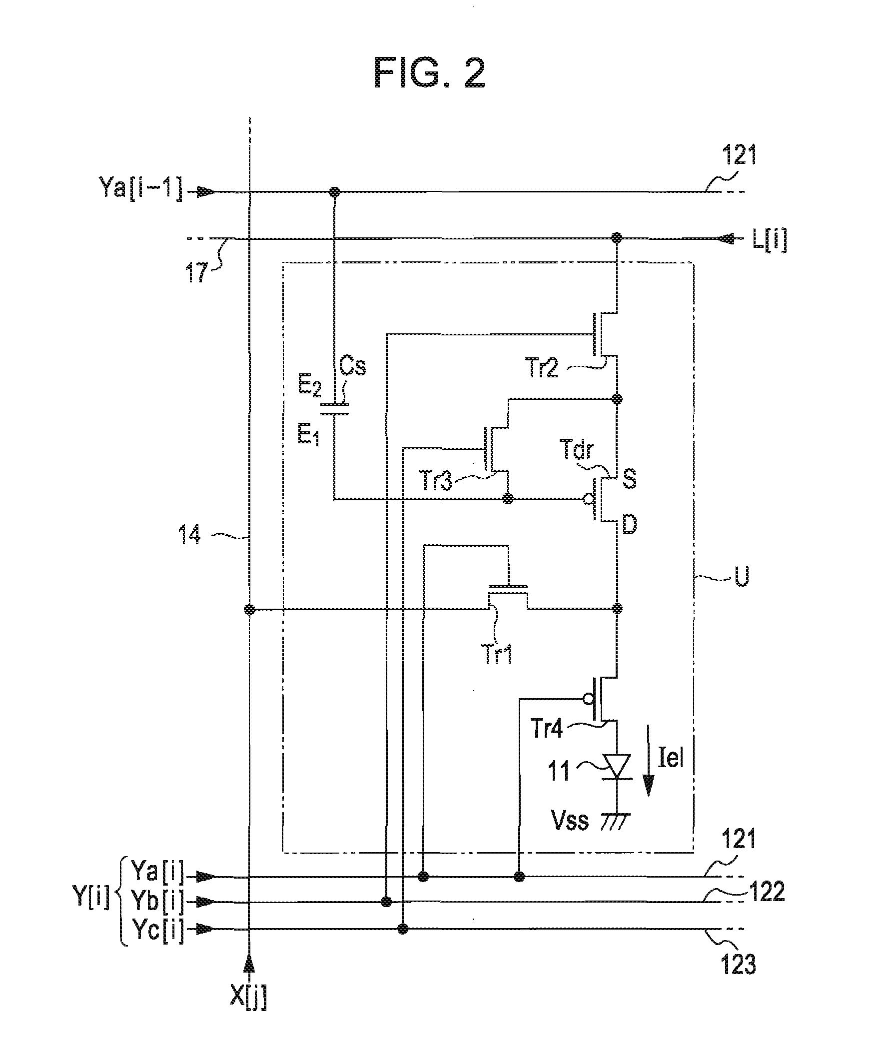
[0060]FIG. 1 is a block diagram showing the configuration of an electronic device according to a first embodiment of the invention. An electronic device D of FIG. 1 is an electro-optical device that is used in various electronic apparatuses as a unit for displaying images. The electronic device D includes an element array portion 10a, in which a plurality of unit circuits U are arranged in a planar manner, a scanning line driving circuit 22 and a data line driving circuit 24 that drive the individual unit circuits U, a voltage control circuit 27 that controls potentials to be supplied to the individual unit circuits U.

[0061] As shown in FIG. 1, in the element array portion 10, m scanning lines 12 extending in an X direction, m potential supply lines 17 extending in the X direction to be in pairs with the scanning lines 12, n data lines 14 extending in a Y direction perpendicular to the X direction are formed (where m and n are natural numbers). The unit circuits U are corresponding...

second embodiment

[0099]FIG. 8 is a block diagram showing the configuration of an electronic device according to a second embodiment of the invention. The electronic device D shown in FIG. 8 is an electro-optical device that is used in various electronic apparatuses as an image display unit. The electronic device D includes an element array portion 10 having a plurality of unit circuits U that are arranged in a planar manner, a scanning line driving circuit 23 and a data line driving circuit 25 that drive each of the unit circuit U, and a voltage control circuit 27 that controls a voltage to be supplied to each of the unit circuits U.

[0100] As shown in FIG. 8, in the element array portion 10, m scanning lines 13 extending in the X direction, m voltage supply lines 17 extending in the X direction to be in pairs with the scanning lines 13, n data lines 15 extending in the Y direction perpendicular to the X direction are formed (where m and n are natural numbers). The unit circuits U are correspondingl...

third embodiment

[0130] Next, an electronic device D according to a third embodiment of the invention will be described. Moreover, in this embodiment, the same parts as those in the second embodiment are represented by the same reference numerals, and the descriptions thereof will be omitted.

[0131]FIG. 15 is a circuit diagram showing the configuration of the unit circuit U according to this embodiment. As shown in FIG. 15, in this embodiment, the conductivity type of the driving transistor Tdr is a p-channel type. The electro-optical element 11 is connected to the drain (D) of the driving transistor Tdr. Moreover, like the second embodiment, each of the terminals of the driving transistor Tdr is switched from one of the source and the drain to the other, but, in this embodiment, for convenience of explanation, the terminal close to the electro-optical element 11 is represented by ‘drain’ and the opposing terminal is represented by ‘source’.

[0132] A transistor Tr1 that controls an electrical connec...


PUM


Abstract

A method of driving an electronic device, which has a driving transistor having a control terminal a first terminal, and a second terminal, a conduction state between the first terminal and the second terminal changing according to a potential of the control terminal, and a unit circuit having a driven element to be driven according to the conduction state of the driving transistor, includes supplying a first potential to a potential supply line in an initialization period, and electrically connecting the potential supply line and the control terminal of the driving transistor to each other, electrically connecting a data line to which a data signal is supplied, and the first terminal of the driving transistor to each other in a writing period after the initialization period, and supplying a second potential different from the first potential to the potential supply line in a driving period after the writing period, and electrically connecting the potential supply line and the second terminal of the driving transistor in the driving period so as to drive the driven element.

Description

BACKGROUND [0001] 1. Technical Field [0002] The present invention relates to a technique for controlling behaviors of various driven elements, such as organic light-emitting diode (hereinafter, referred to as ‘OLED’) elements, liquid crystal elements, electrophoretic elements, electrochromic elements, electron emission elements, resistive elements. [0003] 2. Related Art [0004] Various electronic devices, such as electro-optical devices (light-emitting device) using OLED elements include a plurality of unit circuits that are arranged in a planar manner. Each of the unit circuits has, for example, a transistor (hereinafter, referred to as ‘driving transistor’) whose gate is set to a potential according to a data signal, and a driven element (for example, an OLED element) that is driven by a current flowing in the driving transistor according to the potential of the gate (for example, see '51.4: Invited Paper: Modeling and Design of Polysilicon Drive Circuits for OLED Displays', Simon ...

Claims


Application Information

Patent Timeline
Patent Type & Authority Applications(United States)
IPC IPC(8): G09G3/30
CPCG09G3/22G09G3/3233G09G2300/0465G09G2300/0819G09G2320/043G09G2300/0861G09G2300/0866G09G2300/0876G09G2300/0842G09G3/30G09G3/20
Inventor MIYAZAWA, TAKASHI
Owner SEIKO EPSON CORP
Why Eureka
Try Eureka