Semiconductor memory

Inactive Publication Date: 2007-01-25
SOCIONEXT INC
View PDF6 Cites 11 Cited by
  • Summary
  • Abstract
  • Description
  • Claims
  • Application Information

AI Technical Summary

Benefits of technology

[0057] With the above features, it is possible to store information in the dummy memory cells with small operations to change the load capacitance connected to the dummy read line.

Problems solved by technology

In the semiconductor memory, the timing of activating a sense amplifier is sometimes varied due to the effects of variations in production which occur during formation of memory cell arrays over a silicon substrate, or variations in environmental factors, such as temperature condition, voltage condition, etc., and this variation in timing results in an unstable reading operation.
However, in general, the threshold voltage cannot be decreased so much in view of suppression of drain leakage of transistors.
Therefore, when the semiconductor integrated circuit operates at a low voltage in a process of relatively-high threshold voltage, a variation in transistor performance becomes considerably large.
Thus, when the timing generation function which uses the replica column 550 as in the semiconductor memory 500 operates at a low voltage near a threshold voltage, the transistor capacity of a memory cell can be far smaller than that of a corresponding replica memory cell, causing an error in the operation.
However, this results in a redundant circuit structure and increases the circuit area.

Method used


Image

  • Semiconductor memory
  • Semiconductor memory
  • Semiconductor memory

Examples


embodiment 1

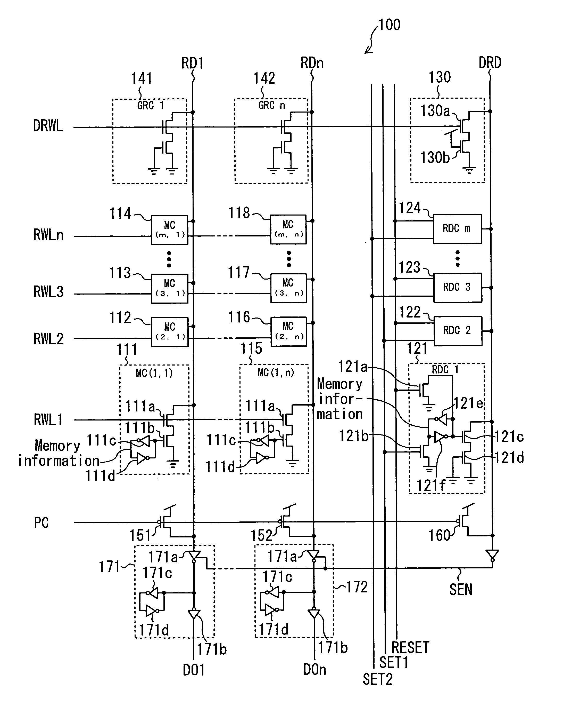
[0093]FIG. 1 is a block diagram showing a structure of a semiconductor memory 100 according to embodiment 1 of the present invention. It should be noted that elements of the circuit relevant to a writing operation are not shown.

[0094] The semiconductor memory 100 includes memory cells (MC) 111 to 118, reset dummy cells (RDC) 121 to 124, a reference cell 130, gate replica cells (GRC) 141 and 142, precharge transistors 151 and 152, a dummy precharge transistor 160, and output circuits 171 and 172.

[0095] The memory cells 111 to 118 have the same structure and are arranged in a matrix of m rows by n columns. The memory cells 111 to 118 each output information stored therein to a read line connected to the memory cell (any one of read lines RD1 to RDn) according to the potential of a read word line connected to the memory cell (any one of read word lines RWL1 to RWLn). In a reading operation, any one of the read word lines RWL1 to RWLn which is selected according to an address signal (...

embodiment 2

[0135]FIG. 4 is a block diagram showing a structure of a semiconductor memory 200 according to embodiment 2 of the present invention. The semiconductor memory 200 is different from the semiconductor memory 100 in that the semiconductor memory 200 includes memory cells 211 to 216 in place of the memory cells 111 to 118 and reset dummy cells 221 to 223 in place of the reset dummy cells 121 to 124 and further includes AND circuits 281 to 283. In the following descriptions of this embodiment, elements having the same functions as those of embodiment 1 are denoted by the same reference numerals, and the descriptions thereof are herein omitted.

[0136] The memory cells 211 to 216 have the same structure and are arranged in a matrix of m rows by n columns. The memory cells 211 to 216 each output information stored therein to a read line connected to the memory cell (any one of read lines RD1 to RDn) according to the potential of a read word line connected to the memory cell (any one of read...

embodiment 3

[0150]FIG. 7 is a block diagram showing a structure of a semiconductor memory 300 according to embodiment 3 of the present invention. As shown in FIG. 7, the semiconductor memory 300 includes an AND circuit 380 in addition to the components of the semiconductor memory 200.

[0151] Due to the addition of the AND circuit 380, the precharge operation by the precharge transistors 151 and 152 is controlled by dummy precharge signal DPC and the potential of the dummy read line DRD.

[0152] An operation of the semiconductor memory 300 having the above-described structure is described with reference to FIG. 8.

[0153]FIG. 8 is a timing chart showing the voltage waveforms of dummy precharge signal DPC, the read word lines RWL1 and RWL2, the dummy read word line DRWL, the dummy read line DRD, the read line RD1, precharge sense amplifier enable signal PSEN (which is the inverse of the dummy read line), and data output DO1 in a reading operation. It should be noted that, in the following descripti...


PUM


Abstract

Reset dummy cells which change the load capacitance of a dummy read line DRD according to stored information are provided. Memory information are set to the reset dummy cells according to environmental factors, such as the temperature condition, voltage condition, etc. The timing of reading data from memory cells is controlled according to a change in voltage of the dummy read line DRD which is caused due to the discharge of the precharged dummy read line DRD.

Description

CROSS-REFERENCE TO RELATED APPLICATIONS [0001] This nonprovisional application claims priority under 35 U.S.C. §119(a) on Japanese Patent Application No. 2005-197881 filed on Jul. 6, 2005, and the entire contents disclosed in the specification, drawings and claims of this application are hereby incorporated by reference. BACKGROUND OF THE INVENTION [0002] 1. Field of the Invention [0003] The present invention relates to a semiconductor memory wherein a bit line is precharged to a predetermined potential for reading data. [0004] 2. Description of the Prior Art [0005] In the semiconductor memory, the timing of activating a sense amplifier is sometimes varied due to the effects of variations in production which occur during formation of memory cell arrays over a silicon substrate, or variations in environmental factors, such as temperature condition, voltage condition, etc., and this variation in timing results in an unstable reading operation. An example of a semiconductor memory desi...

Claims


Application Information

Patent Timeline
IPC IPC(8): G11C7/00G11C7/02
CPCG11C7/227G11C7/22G11C7/04
Inventor SUMITANI, NORIHIKOTSUJIMURA, KAZUKI
Owner SOCIONEXT INC
Why Eureka
Try Eureka