
Electrostatic discharge protection circuit with reduced mounting area and junction capacitance

Inactive Publication Date: 2007-02-01
SK HYNIX INC
View PDF8 Cites 3 Cited by
  • Summary
  • Abstract
  • Description
  • Claims
  • Application Information

AI Technical Summary

Benefits of technology

[0021] Another object of the present invention is to decrease the area occupied by an ESD protection circuit in a semiconductor chip.

Problems solved by technology

Among these, a failure mode due to an electrical overstress and a failure mode due to an electrostatic discharge (hereinafter, the “ESD”) are caused by undesirable electric charges negatively affecting the integrated circuit.
The electrostatic current generated by an ESD phenomenon inside an integrated circuit will concentrate and flow to the weakest portion of a transistor or a junction or a contact or a gate oxide portion in the integrated circuit, and as a result these components are likely to fail (e.g., by melting) during an ESD phenomenon.
The junction capacitance decreases and deteriorates the signal transmission speed and integrity.
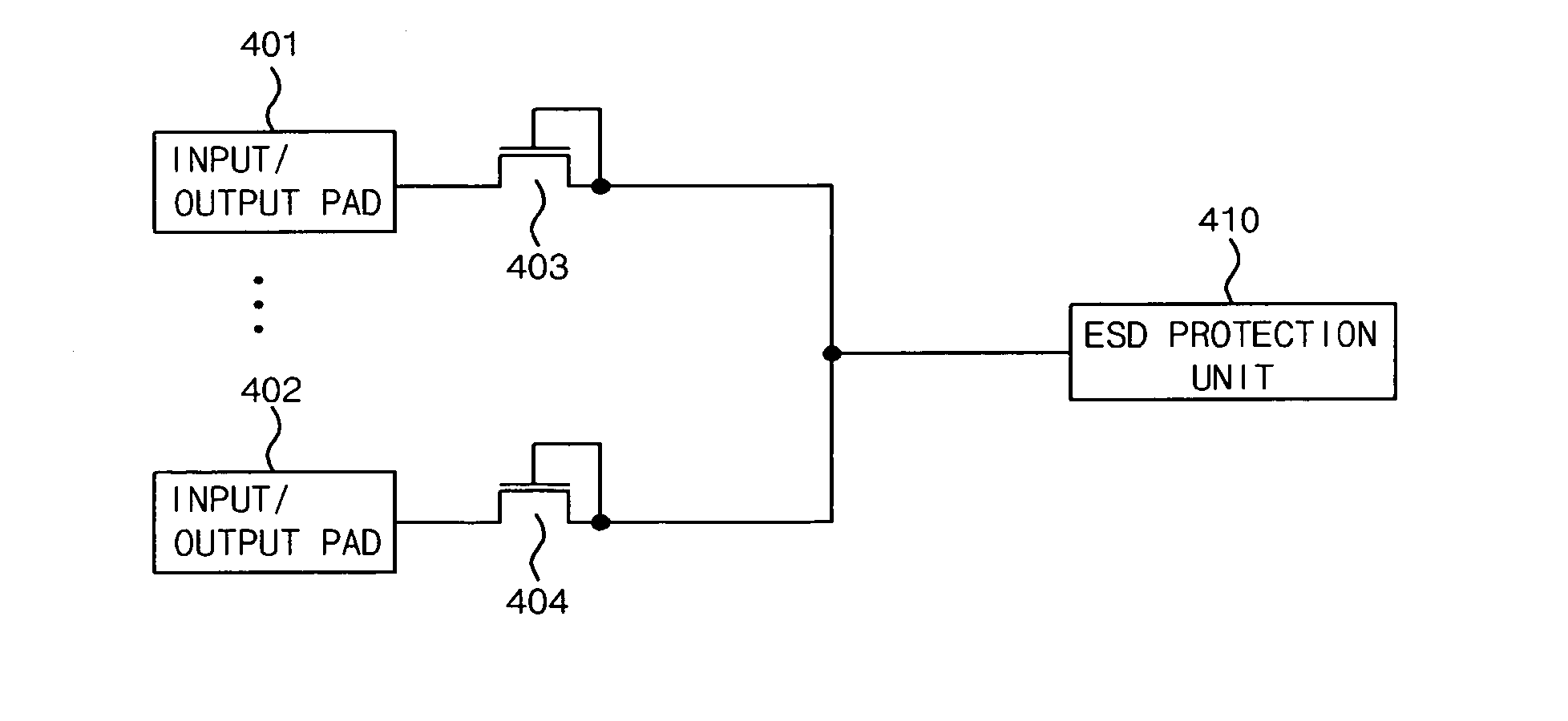
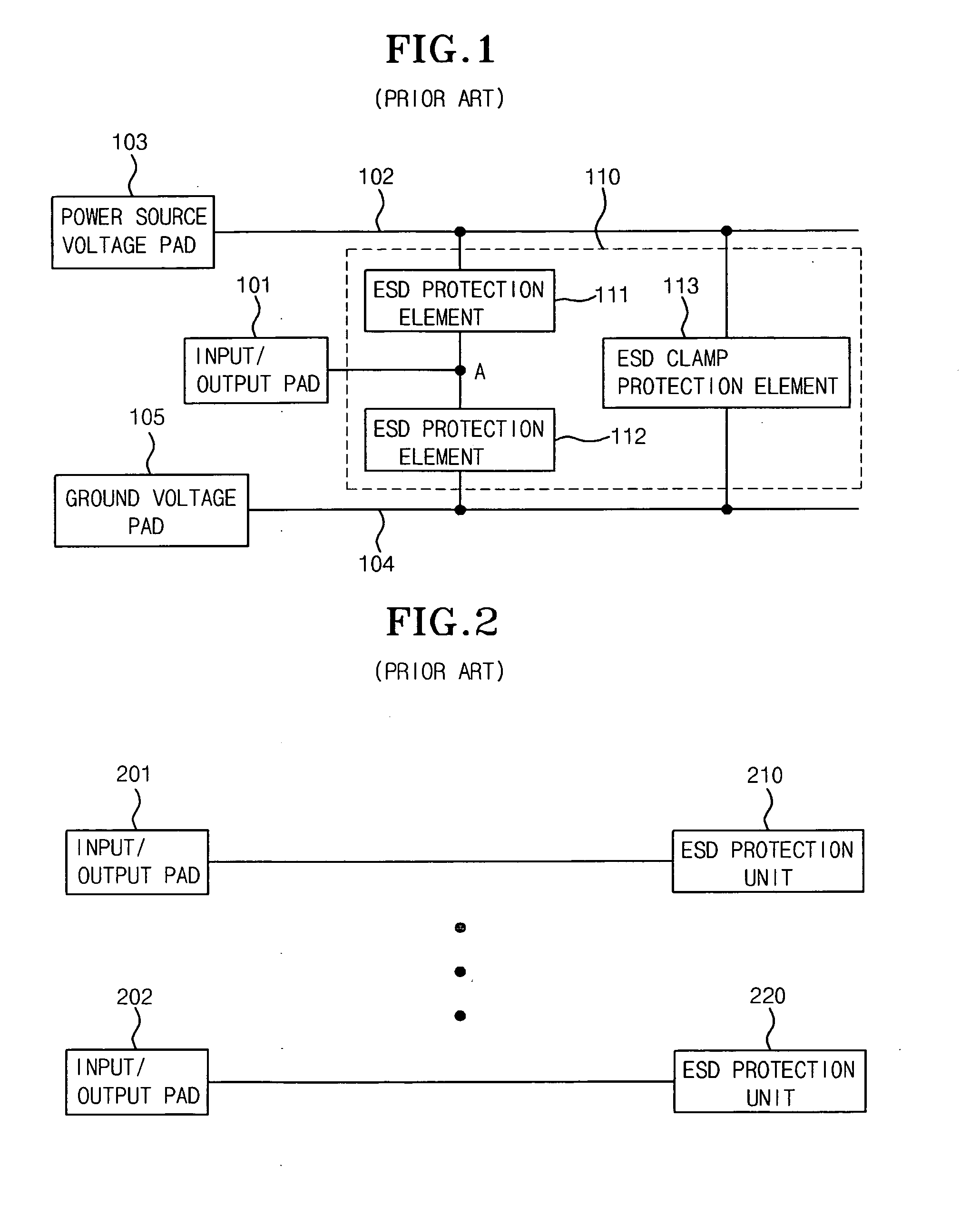
One conventional technique tries to solve this problem by connecting one ESD protection unit (such as 210) to a plurality of input / output pads 201, 202 to decrease the area occupied by the ESD protection circuit; however, as the plurality of input / output pads 201 and 202 are connected to each other via an ESD protection unit, a short can occur and a proper circuit operation cannot be guaranteed.

Method used


Image

  • Electrostatic discharge protection circuit with reduced mounting area and junction capacitance
  • Electrostatic discharge protection circuit with reduced mounting area and junction capacitance
  • Electrostatic discharge protection circuit with reduced mounting area and junction capacitance

Examples


Embodiment Construction

[0035] Reference will now be made in greater detail to a preferred embodiment of the invention, an example of which is illustrated in the accompanying drawings. Wherever possible, the same reference numerals will be used throughout the drawings and the description to refer to the same or like parts.

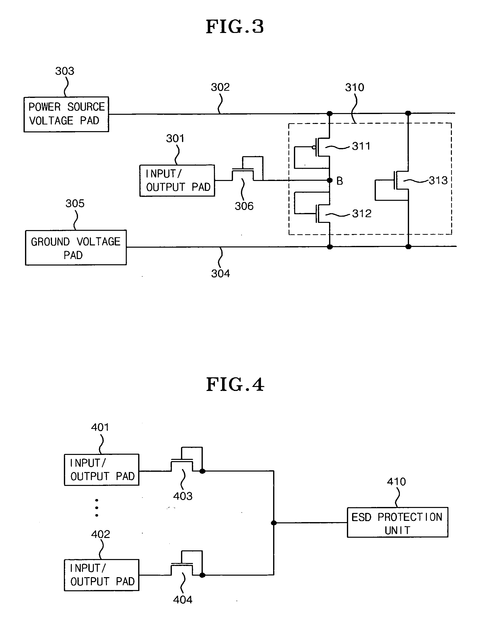
[0036]FIG. 3 is a circuit diagram illustrating an ESD protection circuit in accordance with one embodiment of the present invention.

[0037] Referring to FIG. 3, the ESD protection circuit in accordance with one embodiment of the present invention comprises an input / output pad 301, a power source voltage pad 303 connected to a power source voltage line 302, a ground voltage pad 305 connected to a ground voltage line 304, an ESD protection unit 310 connected between the power source voltage line 302 and the ground voltage line 304, and a switching element 306 connected between the input / output pad 301 and the ESD protection unit 310.

[0038] The ESD protection unit 310 may comprise diodes, ...


PUM


Abstract

The electrostatic discharge protection circuit prevents internal elements from being damaged due to static electricity. The ESD protection circuit includes a first voltage line connected to a power source voltage pad, a second voltage line connected to a ground voltage pad, an ESD protection unit connected between the first voltage line and the second voltage line to provide a static electricity discharge path, and at least one switch connected between an input / output pad and the ESD protection unit to be switched by static electricity.

Description

BACKGROUND OF THE INVENTION [0001] 1. Field of the Invention [0002] The present invention relates, in general, to an electrostatic discharge protection circuit, and more particularly to an electrostatic discharge protection circuit which can prevent internal elements from being damaged due to generation of static electricity. [0003] 2. Description of the Related Art [0004] In general, there are various types of failure modes for the circuits integrated in a semiconductor device. Among these, a failure mode due to an electrical overstress and a failure mode due to an electrostatic discharge (hereinafter, the “ESD”) are caused by undesirable electric charges negatively affecting the integrated circuit. [0005] The ESD occurs due to flowing charges generated by static electricity. The ESD is categorized into a human body model (HBM), a machine model (MM), and a charge device model (CDM) classified based on the source generating the static electricity. [0006] The human body model (HBM), ...

Claims


Application Information

Patent Timeline
IPC IPC(8): H02H9/00
CPCH01L27/0266H01L27/04
Inventor KIM, JANG HOOKWAK, KOOK WHEE
Owner SK HYNIX INC
Learn More