
Decoding Circuit Withstanding High Voltage Via Low-Voltage Mos Transistor And The Implementing Method Thereof

Active Publication Date: 2012-04-19
SHANGHAI HUAHONG GRACE SEMICON MFG CORP
View PDF4 Cites 3 Cited by
  • Summary
  • Abstract
  • Description
  • Claims
  • Application Information

AI Technical Summary

Benefits of technology

[0005]The purpose of the present invention is to provide a decoding circuit withstanding a high voltage via a low-voltage MOS transistor; the decoding circuit has a simple structure and high reliability, an

Problems solved by technology

This will, with area of the device increased inevitably and greatly, not only reduce integration level for the same device area, but also increase circuit complexity and reduce reliability.

Method used


Image

  • Decoding Circuit Withstanding High Voltage Via Low-Voltage Mos Transistor And The Implementing Method Thereof
  • Decoding Circuit Withstanding High Voltage Via Low-Voltage Mos Transistor And The Implementing Method Thereof
  • Decoding Circuit Withstanding High Voltage Via Low-Voltage Mos Transistor And The Implementing Method Thereof

Examples


Embodiment Construction

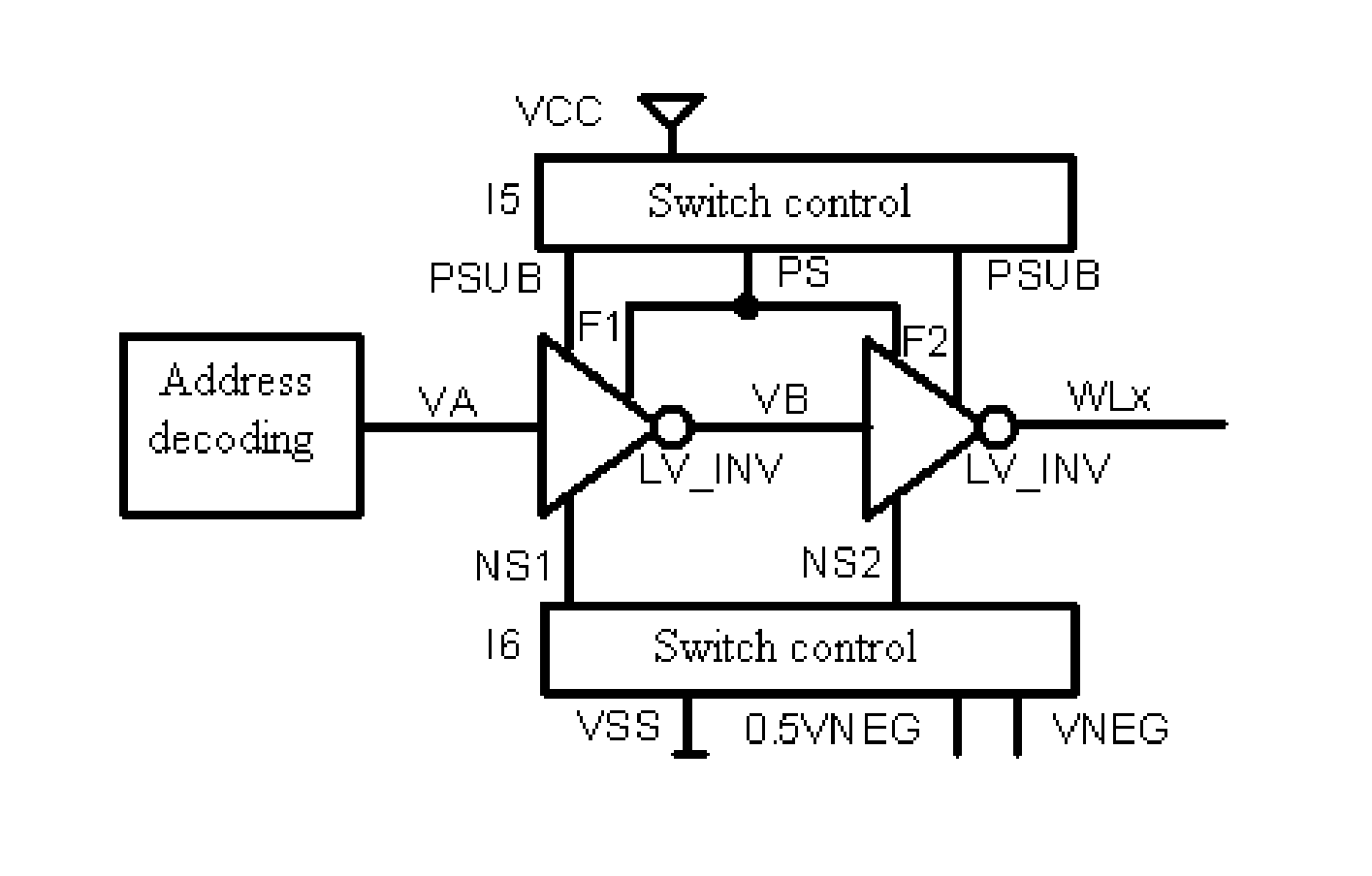
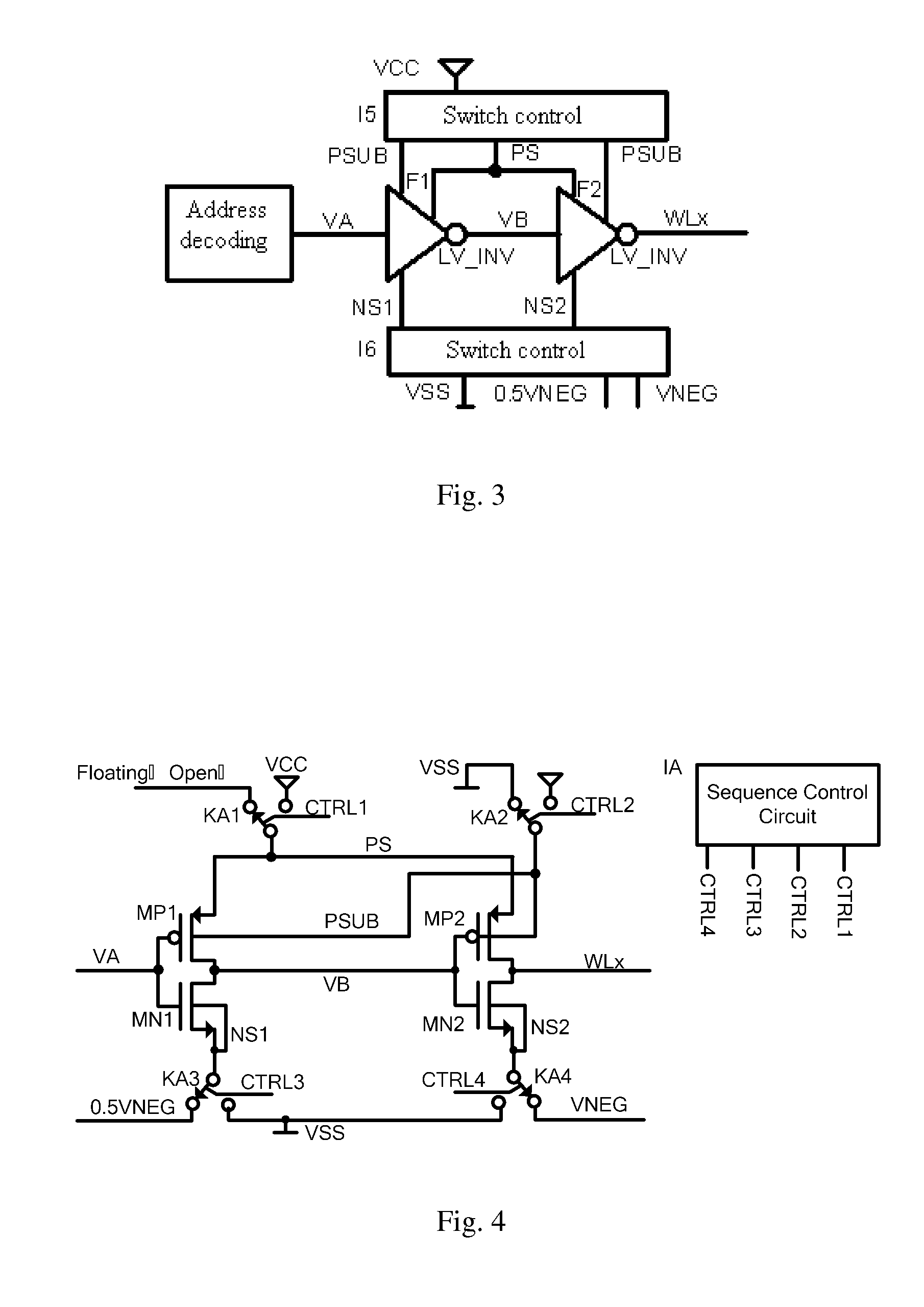
[0026]The designer does not hope to use a high-voltage transistor in the circuit, so as to withstand the high voltage in programming mode and obtain fast decoding output in read mode, and reduce area of the device as well. Therefore, the present invention puts forward a solution, in which a decoding circuit is provided to withstand the high voltage by making use of a low-voltage transistor. As shown in FIGS. 3 and 4, the decoding circuit will be specifically described below by taking a circuit as an example, where two CMOS inverters are connected serially, which can withstand a double negative high voltage. The nominal withstand voltage of the transistor here is smaller than 2 V, while target value of the withstand high voltage (including the negative high voltage and the positive high voltage) is ±4 V.

[0027]The key point of the technical solution of the present invention is as below: Switch the source and the substrate of the two PMOS transistors in the two-stage CMOS inverter to f...


PUM


Abstract

A decoding circuit withstanding high voltage via a low-voltage MOS transistor, where negative high voltage that can be withstood can be as high as double what the transistor itself can withstand via two-stage CMOS inverters connected serially. When the negative high voltage is withstood, the source of a PMOS transistor in the CMOS inverter is switched to high resistance, and the substrate to the ground; the source of an NMOS transistor in the first CMOS inverter is connected with a half negative high voltage, and the source of an NMOS transistor in the second CMOS inverter with a negative high voltage; the first CMOS inverter, whose output is the half negative high voltage, is grounded at its input terminal, and output of the second CMOS inverter is the negative high voltage.

Description

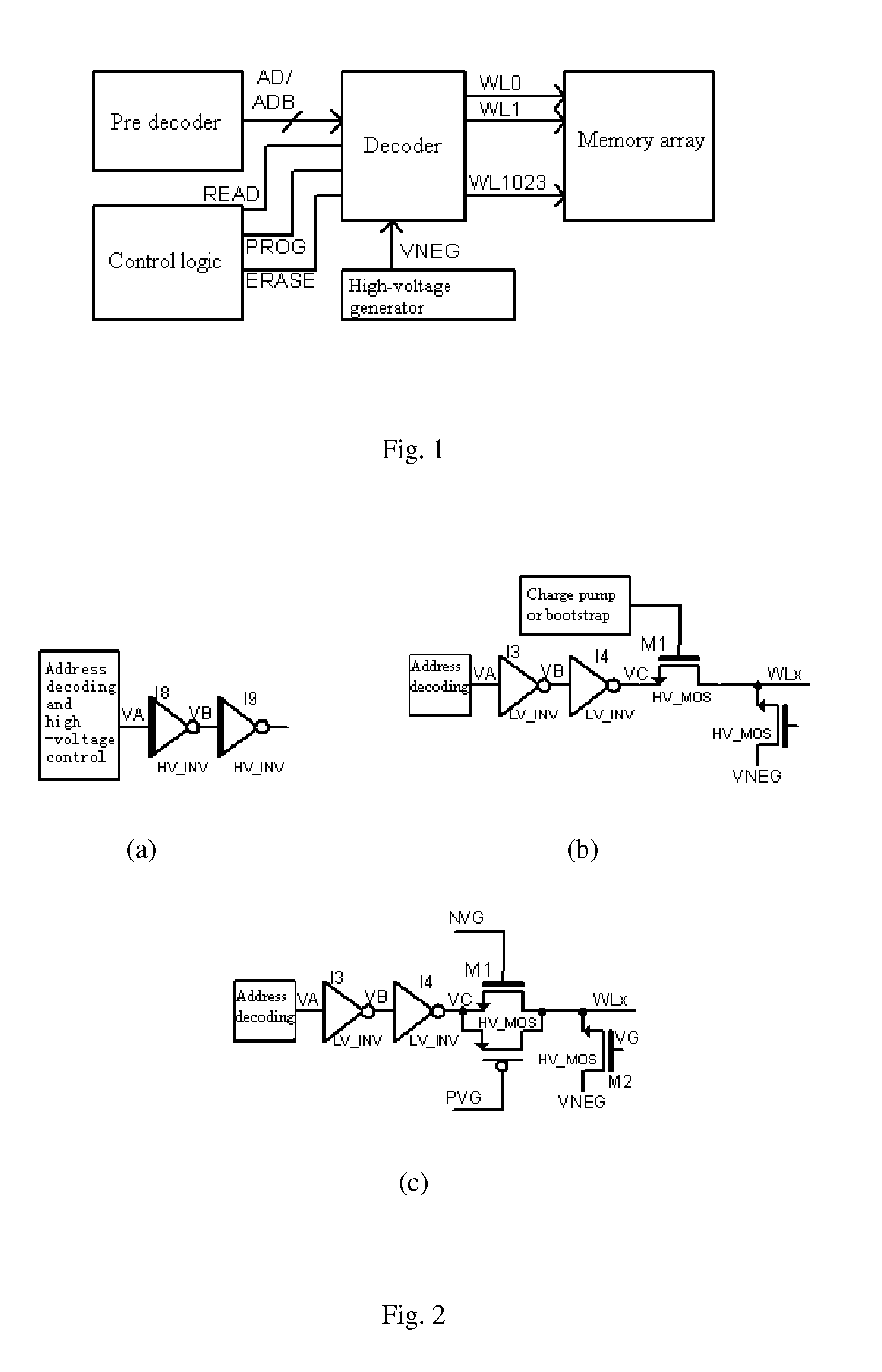
[0001]The current application is a continuation-in-part of, and claims a priority to U.S. Ser. No. 12 / 505,591 filed on Jul. 20, 2009.TECHNICAL FIELD[0002]The present invention relates to the field of the non-volatile memory in the semiconductor integrated circuit, especially to a decoding circuit withstanding a high voltage via a low-voltage MOS transistor; the present invention further relates to a method of implementing the decoding circuit and a memory circuit using the decoding circuit.BACKGROUND TECHNOLOGY[0003]For a word line decoding circuit of such a non-volatile memory as Flash and EEPROM, high-voltage output is required in erasion or programming modes, while fast decoding output in read mode. FIG. 1 is an architecture block diagram of a memory including the word line decoding circuit.[0004]FIG. 2 is word line decoding circuits of three common non-volatile memories. FIG. 2(a) shows withstanding the high voltage by making use of inverters I8 and I9 composed of a high-voltage...

Claims


Application Information

Patent Timeline
IPC IPC(8): H03K19/084
CPCG11C8/08G11C16/10G11C8/10
Inventor WANG, NANFENG, GUOYOU
Owner SHANGHAI HUAHONG GRACE SEMICON MFG CORP
Learn More