
Method of fabricating a ferroelectric stacked memory cell

Inactive Publication Date: 2005-03-29
STMICROELECTRONICS SRL
View PDF8 Cites 3 Cited by
  • Summary
  • Abstract
  • Description
  • Claims
  • Application Information

AI Technical Summary

Benefits of technology

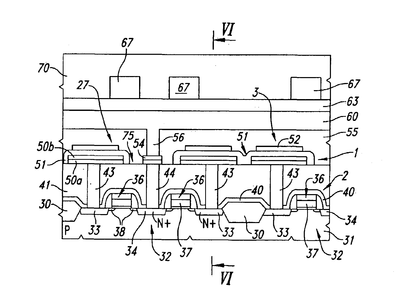
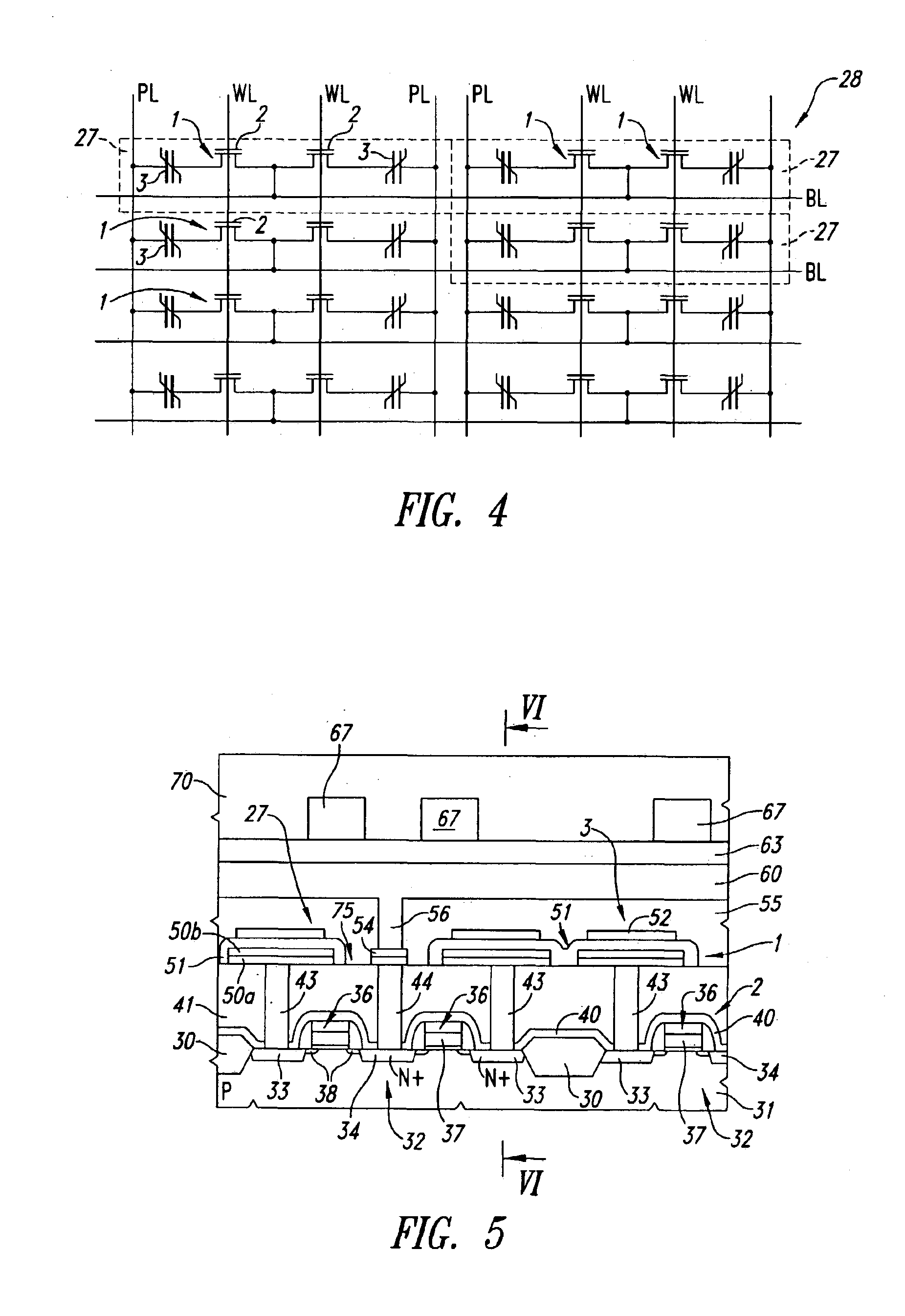
In practice, according to the invention, the dielectric regions of at least two adjacent cells in the direction of the bit lines are no longer separate. In particular, the dielectric region 17 can be continuous and shared between the two adjacent capacitors belonging to pairs of adjacent cells. In this way, the layout definition rules for capacitor scalability are given only by the distance between two lower adjacent electrodes and by the lateral space (enclosure) between upper electrode and lower electrode. This allows, with the same cell area, maximizing the working area of the capacitor compared with the layout of the arrangement where three different masks for definition of the capacitor are used and the dielectric region is divided between adjacent cells in the direction of the bit lines. This causes an increase in signal amplitude (proportional to the active area of the capacitor) supplied by each cell to the sense amplifier during reading. Alternatively, it is possible to obtain a reduction in the area occupied by the ferroelectric cells.

Problems solved by technology

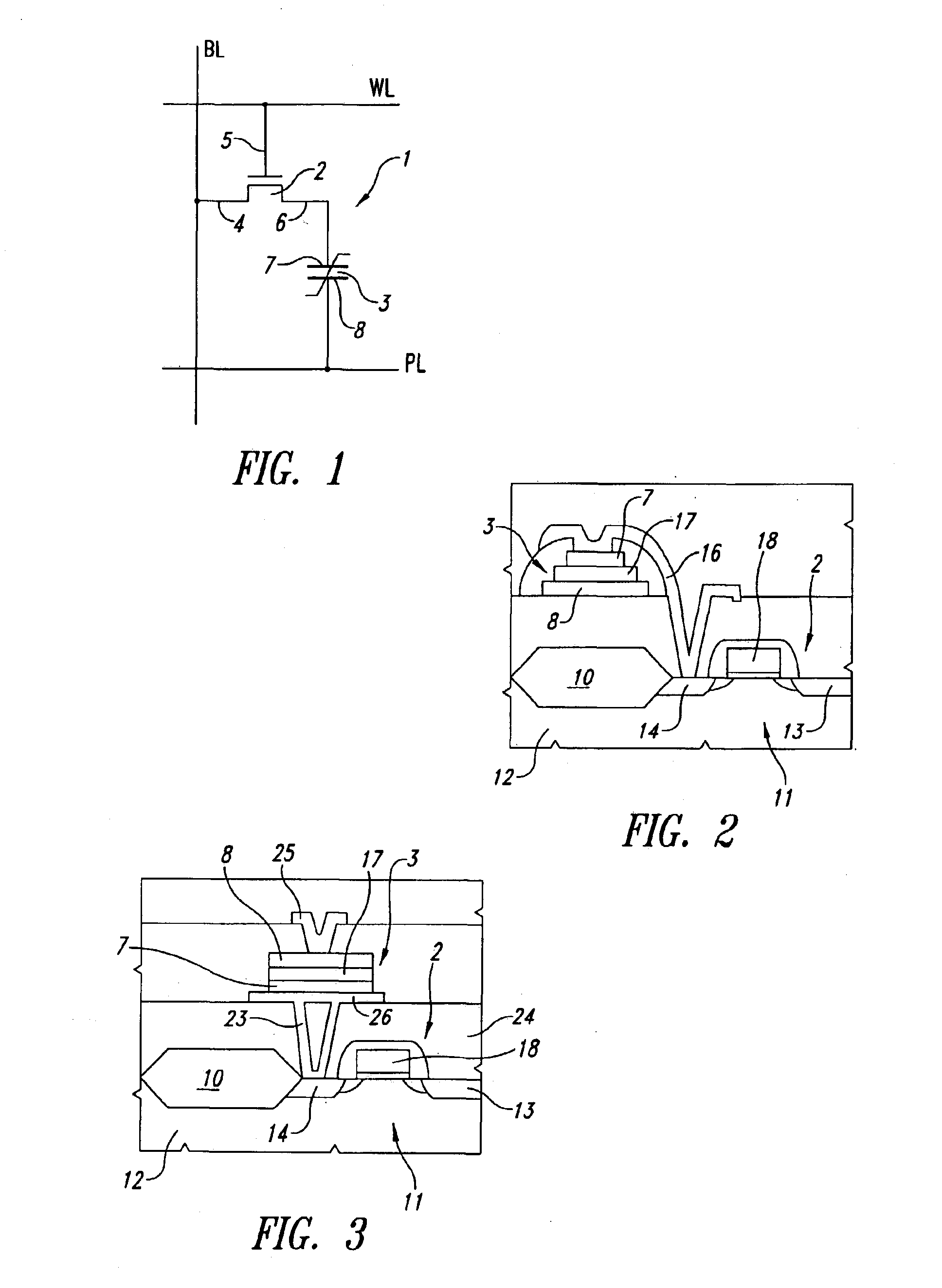
In all these cases, the connection of at least one of the plates 7,8 with the same mask used for the connection of the ferroelectric material composing the dielectric region 17 is critical; for example, during connection, slightly volatile components are formed, and these can be redeposited along the capacitor edge and damage its active zone, causing a decay in the ferroelectric properties of the capacitor, with an increase in edge losses and lower voltage strength.

Method used


Image

  • Method of fabricating a ferroelectric stacked memory cell
  • Method of fabricating a ferroelectric stacked memory cell
  • Method of fabricating a ferroelectric stacked memory cell

Examples


Embodiment Construction

FIGS. 5-7 show stacked cells 1 constructed according to the invention. The present description refers to ferroelectric cells in particular, without being restricted to these.

In detail, FIG. 5 shows a pair of cells 27 and a single ferroelectric cell 1 adjacent to the pair of cells 27 in the direction of the bit lines (horizontal direction in FIG. 5). Pairs of adjacent cells 27 are insulated from each other by a thick oxide layer 30 (field oxide) which delimits, inside a P-type substrate 31, active areas 32 in which two drain regions 33 and a common N+ type source region 34 are formed. In a known way, gate electrodes 36 are formed above the substrate 31 and are insulated therefrom by a thin oxide layer 37. The gate electrodes 36 are preferably made by bands comprising a double layer of polycrystalline silicon and tungsten silicide running perpendicular to FIG. 5 and defining word lines; the gate electrodes 36 are also laterally flanked by oxide spacers 38.

Less doped drain extension re...


PUM


Abstract

The cells of the stacked type each comprise a MOS transistor formed in an active region of a substrate of semiconductor material and a capacitor formed above the active region; each MOS transistor has a first and a second conductive region and a control electrode and each capacitor has a first and a second plate separated by a dielectric region material, for example, ferroelectric one. The first conductive region of each MOS transistor is connected to the first plate of a respective capacitor, the second conductive region of each MOS transistor is connected to a respective bit line, the control electrode of each MOS transistor is connected to a respective word line, the second plate of each capacitor is connected to a respective plate line. The plate lines run perpendicular to the bit line and parallel to the word lines. At least two cells adjacent in a parallel direction to the bit lines share the same dielectric region material and the same plate line. In this way, the manufacturing process is not critical and the size of the cells is minimal.

Description

BACKGROUND OF THE INVENTION1. Field of the InventionThe present invention refers to a stacked type of memory cell structure. In particular, the memory cell described is of the ferroelectric non-volatile type, but the same structure can be used for DRAM cells.2. Description of the Related ArtAs is known and shown in FIG. 1, a ferroelectric cell 1 is composed of a MOS transistor 2 and a capacitor 3 having, as a dielectric, a ferroelectric material, for example PZT (PbZr1-xTixO3, perovskite) or SBT (SrBi2Ta2O9, layered perovskite). In detail, in the ferroelectric cell 1, the NMOS-type transistor 2 has a source terminal 4 connected to a bit line BL, a gate electrode 5 connected to a word line WL and a drain terminal 6 connected to a first plate 7 of the capacitor 3. A second plate 8 of the capacitor 3 is connected to a plate line PL.The cell is capable of storing binary information thanks to the hysteresis characteristics of the ferroelectric material which is sandwiched between the pla...

Claims


Application Information

Patent Timeline
IPC IPC(8): H01L21/70H01L27/115H01L21/8246H01L21/8242H01L27/108
CPCH01L27/11507H01L27/11502H01L27/115H01L27/10811H01L27/10888H10B12/312H10B12/485H10B53/30H10B69/00H10B53/00
Inventor DEMANGE, NICOLASZAMBRANO, RAFFAELE
Owner STMICROELECTRONICS SRL
Learn More