Flash memory device capable of storing multi-bit data and single-bit data

a flash memory and data storage technology, applied in the field of flash memory devices, can solve the problems of increasing system memory costs, eventual destruction of tunnel oxide layers,

Active Publication Date: 2007-02-01
SAMSUNG ELECTRONICS CO LTD
View PDF4 Cites 75 Cited by
  • Summary
  • Abstract
  • Description
  • Claims
  • Application Information

AI Technical Summary

Benefits of technology

[0033] In below, a nonvolatile memory device is used as one example for illustrating characteristics and functions of the present invention. However, those skilled in the art may easily understand other advantages and performance of the present invention according to contents described herein

Problems solved by technology

Further, the repetition of program/erase cycles can stress the tunnel oxide layer at the bottom of a cell transistor's floating gate, which can result in the eventual destruction of the tunnel oxide layer.
Additional problems can also arise

Method used


Image

  • Flash memory device capable of storing multi-bit data and single-bit data
  • Flash memory device capable of storing multi-bit data and single-bit data
  • Flash memory device capable of storing multi-bit data and single-bit data

Examples


first embodiment

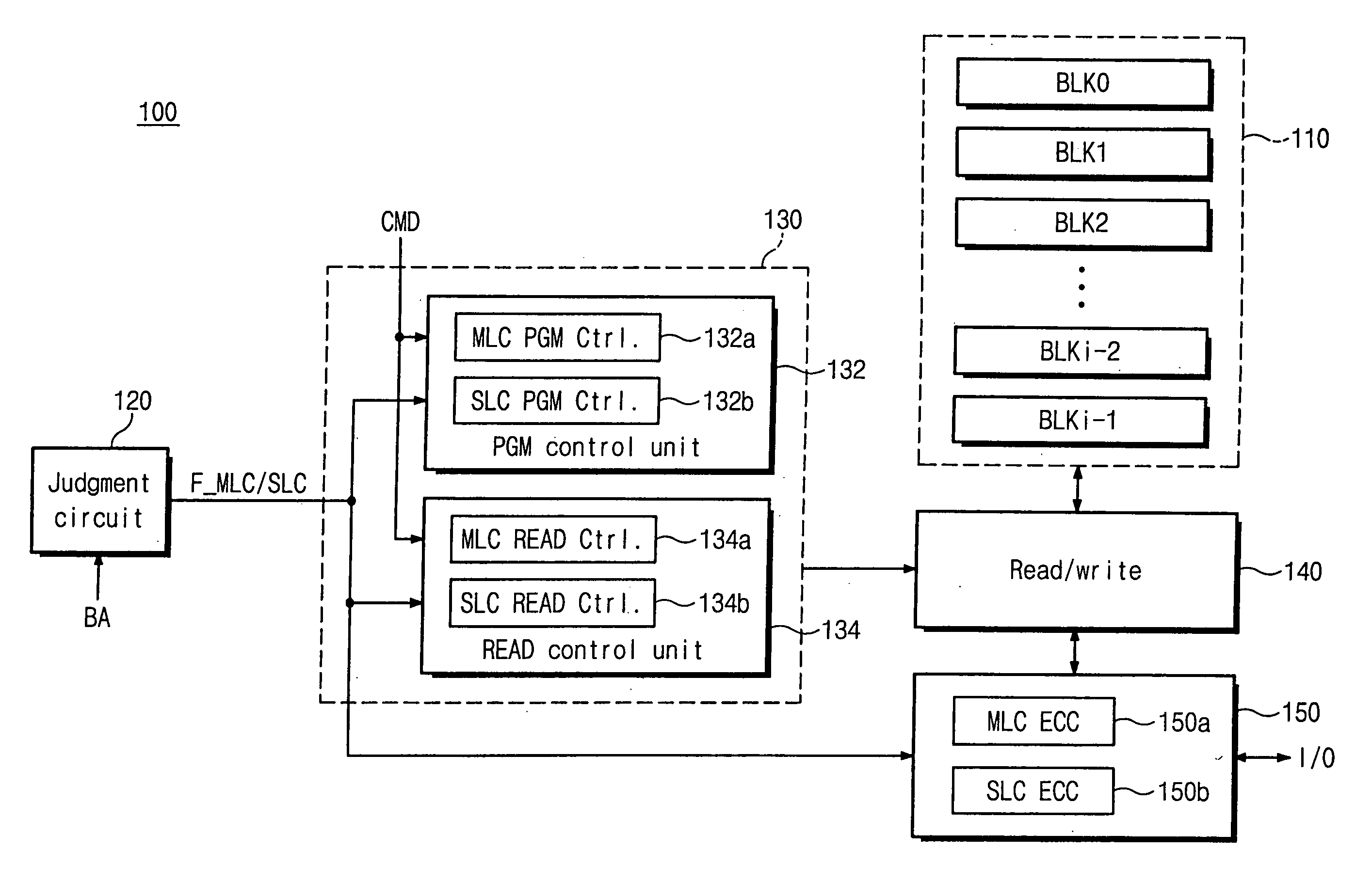
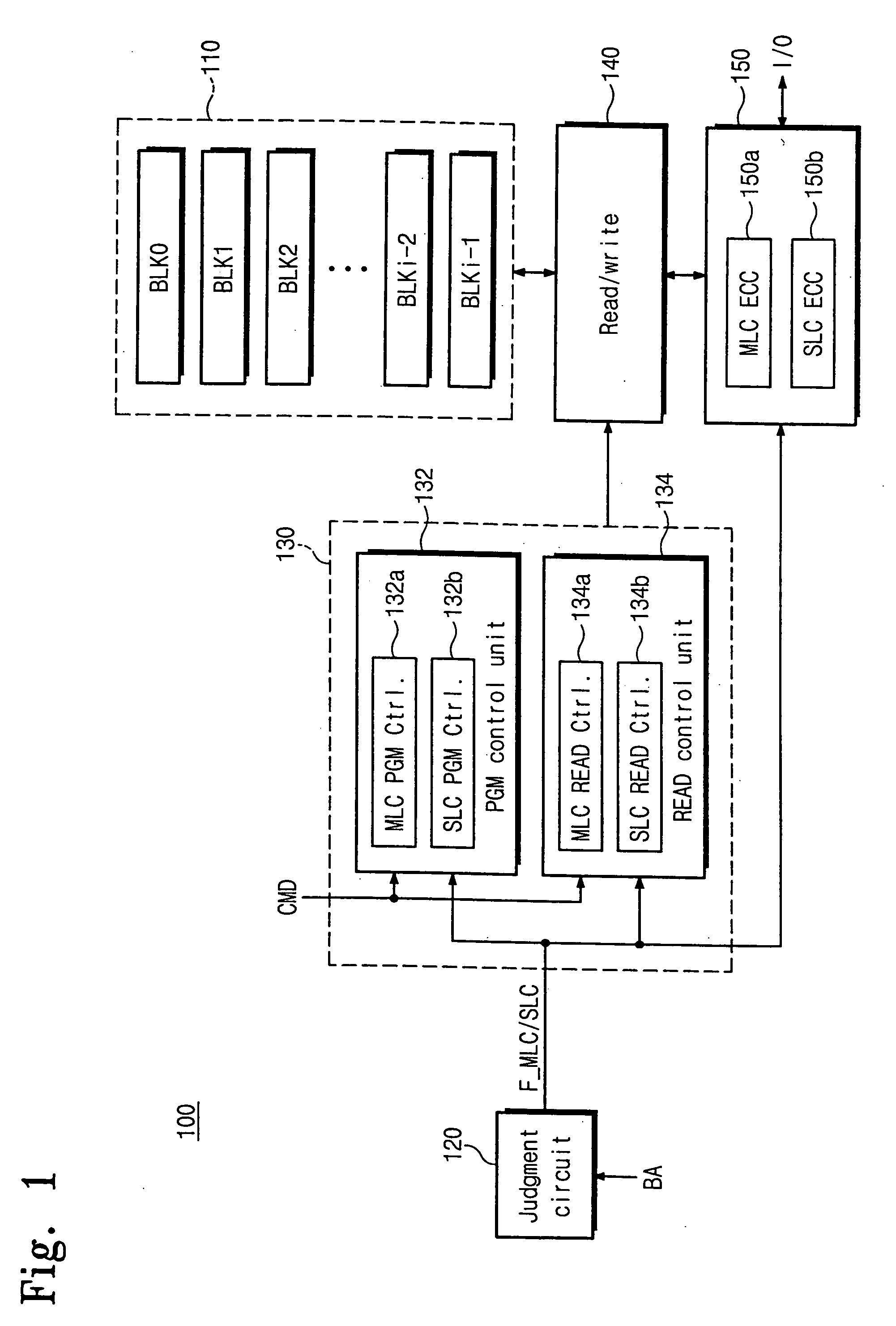
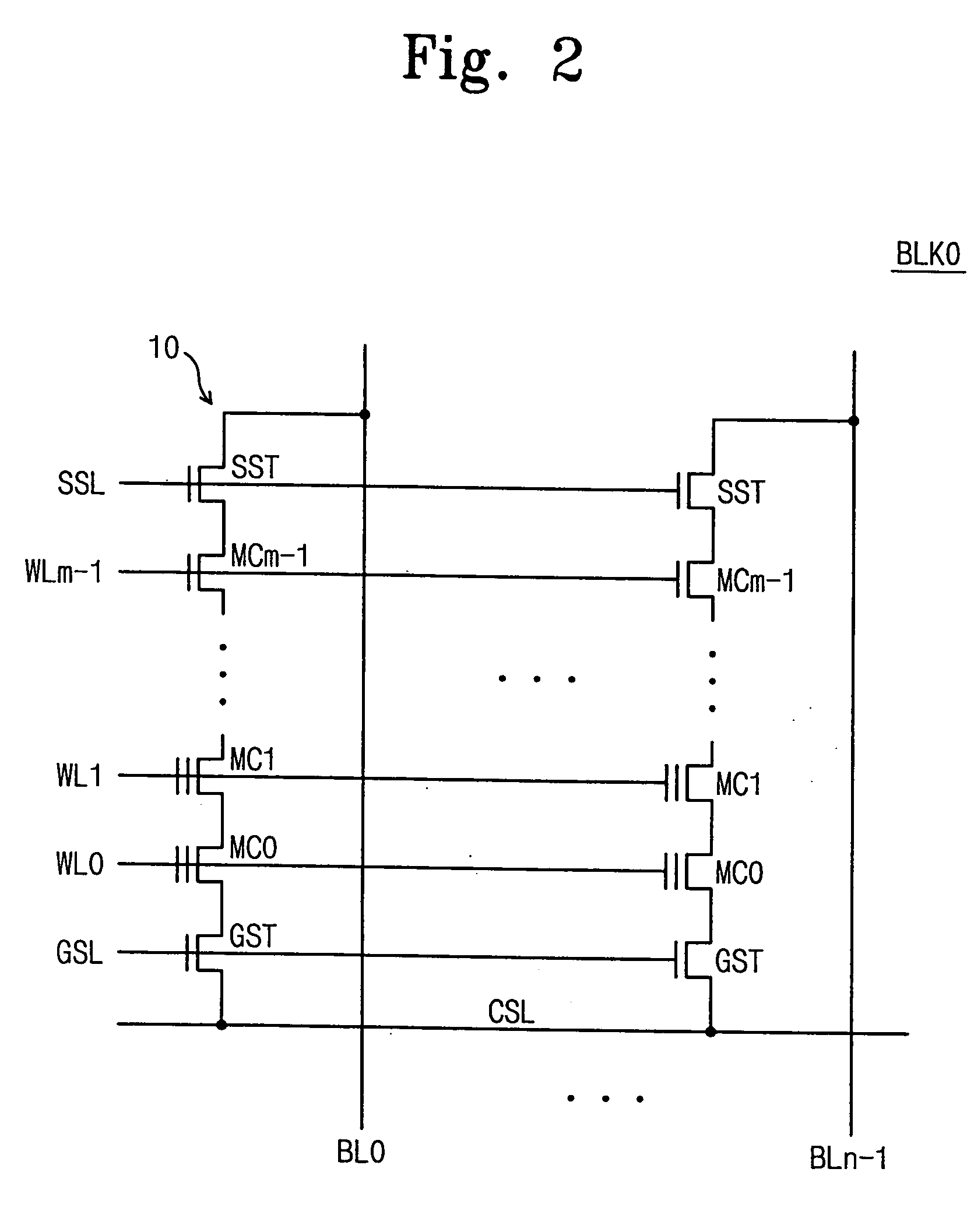
[0048]FIG. 1 is a block diagram of a flash memory device 100 according to the preset invention. As shown in FIG. 1, the flash memory device 100 can include a memory cell array 110 that can include a plurality of memory blocks BLK0˜BLKi-1 with the memory blocks BLK0˜BLKi-1 classified into two groups: a first group used to store single-bit data, and a second group used to store multi-bit data. The memory blocks BLK0˜BLKi-1 can share a common configuration, of which one such memory block (BLK0) is depicted in FIG. 2.

[0049] Referring to FIG. 2, the exemplary memory block BLK0 can include a plurality of “cell strings”10 (also known as “NAND strings”) with each cell string corresponding to respective bit lines BL0˜BLn-1. Each cell string 10 can include a “string select transistor” SST, a “ground select transistor” GST and a plurality of memory cells MCm-1˜MC0 connected in series between the select transistors SST and GST. Each string select transistor SST has a drain connected to a corres...

second embodiment

[0070]FIG. 4 is a block diagram illustrating the judgment circuit 120 of FIG. 1 according to the present invention, and FIG. 5 is a circuit diagram illustrating a portion of a register of FIG. 4.

[0071] Referring to FIG. 4, the judgment circuit 120 can include a decoder 121, a registers 123, and a selector 125. The decoder 121 can decode a register address A_REG inputted from an external device in a power-up mode, and activate one select line among a plurality of select lines. The number of the select lines is equal to the number of the memory blocks BLK0˜BLKi-1 in the memory cell array 110 of FIG. 1.

[0072] The registers 123 can operate in response to the output of the decoder 121, and can be used for storing multi-bit / single-bit region information of the memory blocks BLK0˜BLKi-1 of the memory cell array 110, e.g., MLC / SLC information indicating whether or not a particular memory block is part of a multi-bit data region. The registers 123 include a plurality of register regions (co...

third embodiment

[0087]FIG. 7 is a block diagram showing a flash memory device 200 according to the present invention. As shown in FIG. 7, the flash memory device 200 can include a memory cell array 210, a judgment circuit 220, a power-up reset (POR) circuit 230, a bootloader 240, control logic 250, a read / write control circuit 260 and an ECC circuit 270.

[0088] The memory cell array 210 has a plurality of memory blocks BLK0˜BLKi-1 and at least one One-Time-Programmable (OTP) block 211. Each of the memory blocks BLK0˜BLKi-1 may be configured identically to that illustrated in FIG. 2. The memory blocks BLK0˜BLKi-1 can be divided into two groups with the first group used to store single-bit data and the second group used to store multi-bit data. MLC / SLC information, which can include block addresses for appointing first and final memory blocks for storing single-bit (or alternatively multi-bit) data, may be stored in the OTP block 211 of the memory cell array 210.

[0089] The judgment circuit 220 can be...


PUM


Abstract

There is provided a flash memory device capable of manipulating multi-bit and single-bit data. The flash memory device can include a memory cell array with a plurality of memory blocks. The flash memory device can also include a judgment circuit for storing multi-bit/single-bit information indicating whether each of the memory blocks is a multi-bit memory block or not, determining whether or not a memory block of an inputted block address is a multi-bit memory block according to the stored multi-bit/single-bit information and outputting an appropriate flag signal. A read/write circuit for selectively performing multi-bit and single-bit read/program operations of the memory block corresponding to the block address is also included, as well as control logic for controlling the read/write circuit such that the read/write circuit can perform multi-bit or single-bit read/program operations based on the flag signal. An error checking and correction (ECC) circuit including a multi-bit ECC unit and a single-bit ECC unit for checking and correcting an error in a data of the read/write circuit can also be included.

Description

BACKGROUND OF THE INVENTION [0001] 1. Field of the Invention [0002] The present invention relates to memory devices, and more particularly to nonvolatile memory devices having single-bit and multi-bit storage regions. [0003] 2. Description of the Related Art [0004] Market forces have dictated a gradual demand increase for high-capacity memory devices that don't require periodic refresh. A NAND flash memory device is a nonvolatile memory device which provides the large capacity, high integrity and ease of use demanded by consumers. Since NAND flash memories retain data even if a power is turned off, NAND flash memory devices are well-suited for certain electronic devices, such as mobile terminals, mobile computers, and so forth, where a power supply can be abruptly interrupted. [0005] As is well known in the flash-memory semiconductor industry, the data-retention characteristics and the number of program / erase cycles of flash memories are primarily related to the reliability of the f...

Claims


Application Information

Patent Timeline
IPC IPC(8): G11C16/04
CPCG11C11/5621G11C2211/5641G11C16/0483G11C16/04G11C16/10
Inventor LEE, JIN-YUB
Owner SAMSUNG ELECTRONICS CO LTD
Why Eureka
Try Eureka