Display panel

Inactive Publication Date: 2007-02-08
HITACHI DISPLAYS
View PDF13 Cites 0 Cited by
  • Summary
  • Abstract
  • Description
  • Claims
  • Application Information

AI Technical Summary

Benefits of technology

[0027] An effect obtained by the typical aspect of the invention disclosed in the present application is briefly explained as follows.
[

Problems solved by technology

However, since there are problems that it is difficult to manufacture, dispose, and assemble a spacer which is thin enough to be invisible from the outside, and that the spacer is charged up to become the cause of disturbing an image, a display panel structure without a spacer or with fewer spacers is desired.
However, in a large screen panel exceeding 32 inches for example, the display panel itself becomes very heavy.
Further, since a production process of the electron sources is delicate, it is necessary to us

Method used


Image

  • Display panel
  • Display panel
  • Display panel

Examples


Example

[0034] An embodiment of the present invention will now be described in detail with reference to the drawings. In all of the drawings for explaining the embodiment of the present invention, components having the same functions are assigned with the same reference numerals and characters, and thus the redundant explanation thereof will be omitted.

[0035] FIGS. 1 to 4 are views according to a display panel of one embodiment of the present invention,

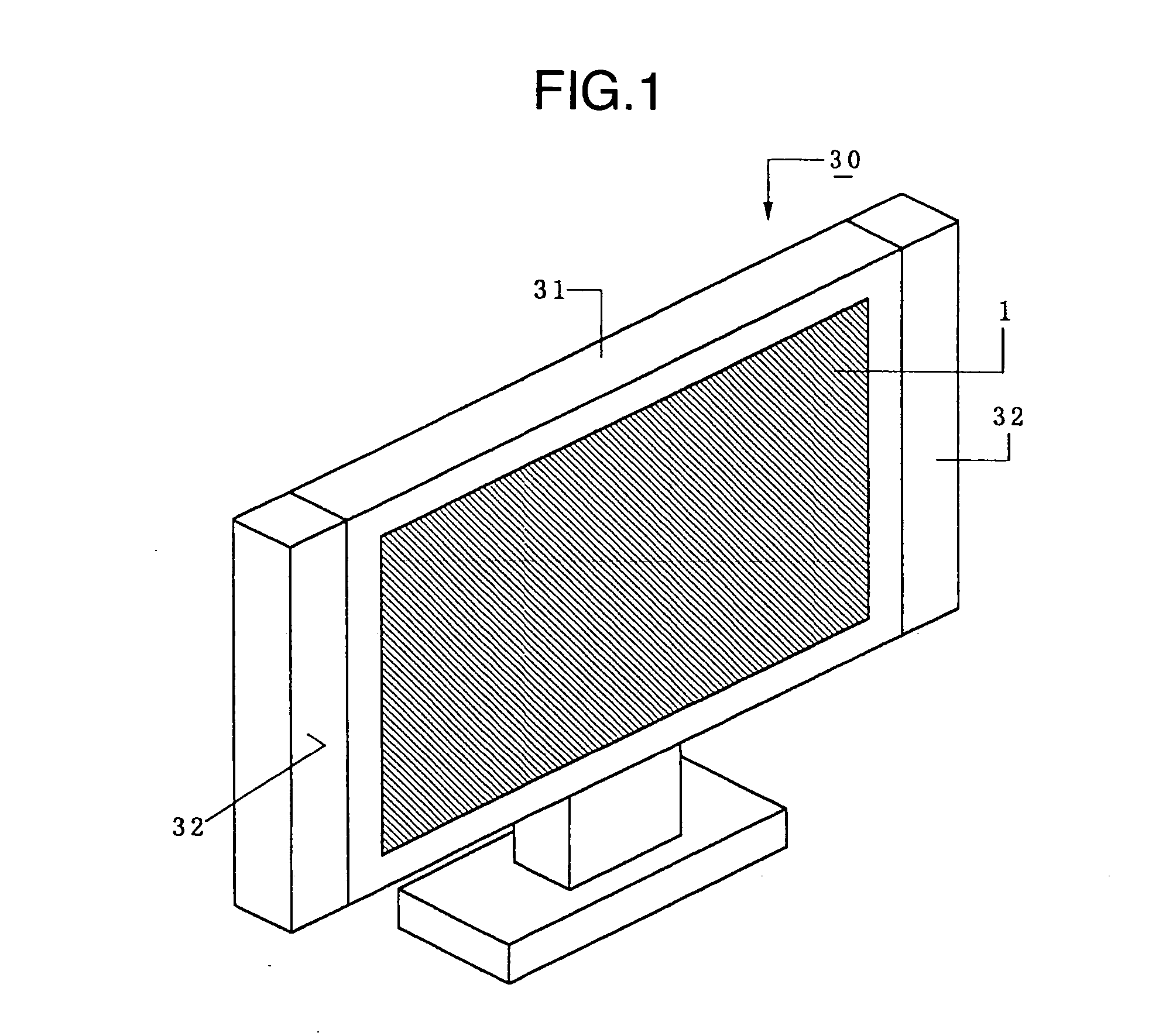
[0036]FIG. 1 is a schematic perspective view showing an external structure of a display apparatus into which the display panel is incorporated,

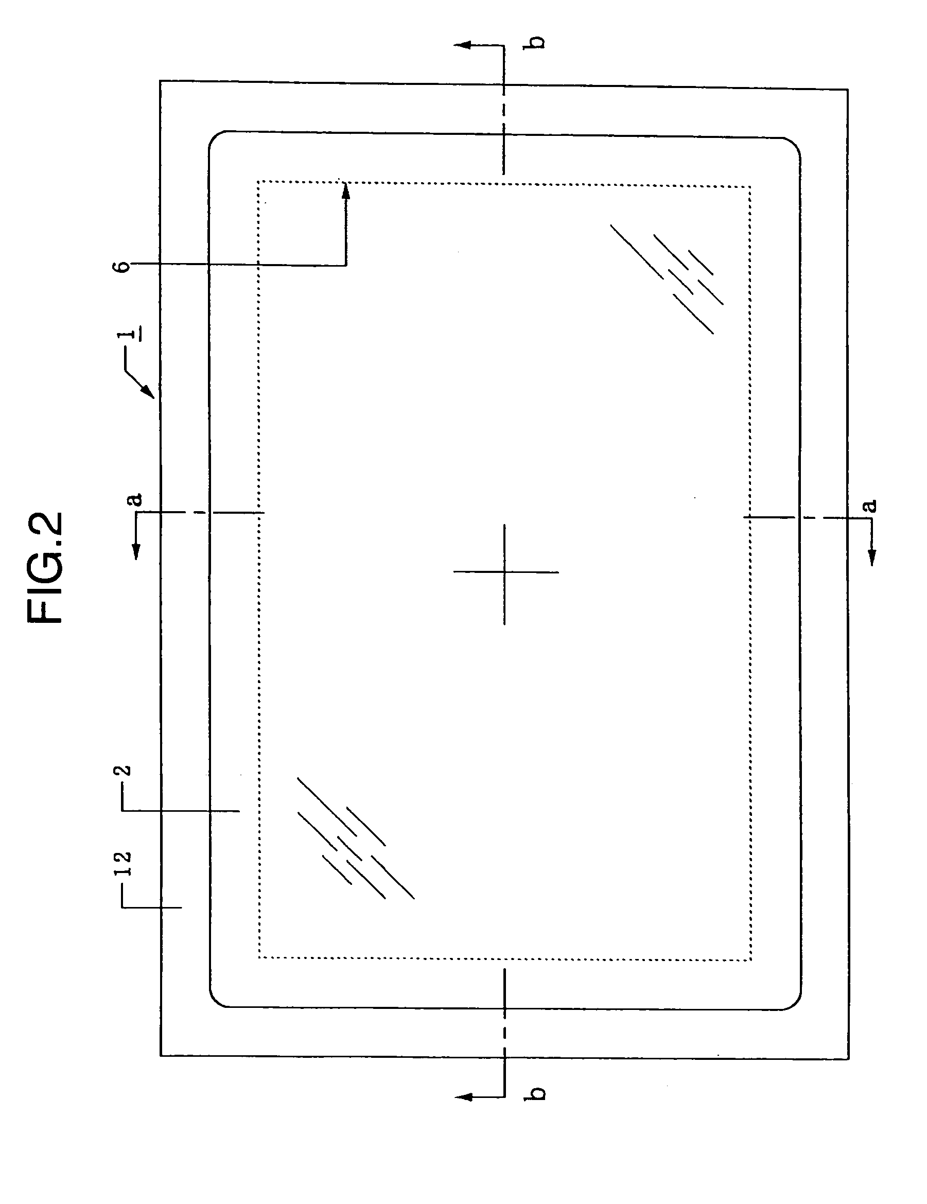
[0037]FIG. 2 is a schematic plane view showing the external structure of the display panel,

[0038]FIGS. 3A and 3B are views showing an internal structure of the display panel (FIG. 3A is a schematic sectional view taken along the line a-a in FIG. 2, and FIG. 3B is a schematic sectional view taken long the line b-b in FIG. 2), and

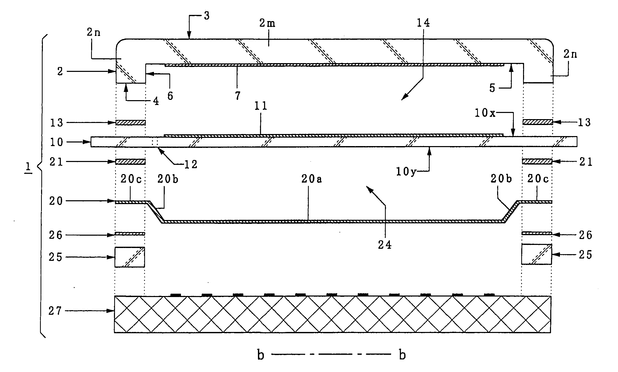
[0039]FIG. 4 is a developed view of FIGS. 3A and 3B.

[0040] In FIG. 4,...


PUM


Abstract

A display panel excellent in reduction in weight and excellent in reliability is provided. The display panel of the invention includes a cover member having a peripheral part bonded and secured to a back surface of a cathode panel, and a central part enclosed by the peripheral part which central part is joined to a reinforcing panel. The reinforcing panel is pressed against a peripheral part of the cathode panel via a support frame by atmospheric pressure exerted on the cover member.

Description

BACKGROUND OF THE INVENTION [0001] 1. Field of the Invention [0002] The present invention relates to a display panel, and more particularly to an art effective when applied to a field emission display (FED: Field Emission Display) panel. [0003] 2. Description of Related Art [0004] A field emission display panel has the structure in which a cathode panel with a number of electron sources for emitting electrons formed thereon is disposed so as to be opposed to an anode panel coated with a phosphor via a gap, so that the electrons emitted from the electron source corresponding to each pixel hits against the phosphor to emit light to display an image. [0005] The basic structure of a field emission display panel is described in “Feature article: Basic Knowledge of Electronic Display for Young Engineers” on pages 94-102 of “Electronic Material” published in April, 2004 by Kogyo Chosakai Publishing Co., LTD, (hereinafter referred to as Non-patent Document 1), for example. [0006] Further, a...

Claims


Application Information

Patent Timeline
IPC IPC(8): H01J63/04H01J1/62
CPCH01J29/862H01J31/123H01J29/87
Inventor KAZAMA, ATSUSHINAGATA, TATSUYAKITADA, TAKAAKINAITOU, TAKASHISAWAI, YUICHI
Owner HITACHI DISPLAYS
Why Eureka
Try Eureka