Analog-to-Digital Conversion Method, Analog-to-Digital Converter, Semiconductor Device for Detecting Distribution of Physical Quantity, and Electronic Apparatus

a conversion method and digital converter technology, applied in the field of analog-to-digital conversion methods, can solve the problems of increasing circuit area, increasing noise or power consumption due to data transfer, etc., and achieve the effect of avoiding noise or increase in avoiding noise, current or power consumption, and reducing line length

Active Publication Date: 2007-02-08
SONY CORP
View PDF2 Cites 14 Cited by
  • Summary
  • Abstract
  • Description
  • Claims
  • Application Information

AI Technical Summary

Benefits of technology

[0051] Specifically, a memory for storing the result of the first reading operation and a memory for storing the result of the second reading operation need to be provided (i.e., two memories are needed) separately from the counter. Signal lines for transferring n-bit count values from the counter to the memories are also needed. Moreover, 2 n-bit (double) signal lines are needed for n bits in order to transfer the count values of the first and second counting operations to the subtractor. Thus, the circuit size and the circuit area are increased, and an increase in noise, current consumption, or power consumption is also caused.
[0101] When comparison and counting are performed on a reference component, by starting comparison and counting after resetting the comparator to an operational reference value for reading the reference component, the operating point of the comparator is set at a read potential of the signal, leading to less susceptibility to variations in the reference component. When comparison and counting are performed on a signal component, by starting comparison and counting without resetting the comparator, substantial subtraction can performed by performing the two processes. Therefore, the fixed offset noise, as well as kTC noise, can be removed.

Problems solved by technology

Thus, two n-bit latches are needed for an n-bit signal (2 n latches are needed for each bit), which thus causes an increase in circuit area (hereinafter referred to as a first problem).
Furthermore, in order to subtract the count value of the first counting operation from the count value of the second counting operation before the output circuit 28 outputs a signal to the outside, 2 n signal lines for transferring the count values to the n-bit subtractor circuit 29 of the output circuit 28 are needed, leading to concern for an increase in noise or power consumption due to data transfer (hereinafter referred to as a fourth problem).

Method used


Image

  • Analog-to-Digital Conversion Method, Analog-to-Digital Converter, Semiconductor Device for Detecting Distribution of Physical Quantity, and Electronic Apparatus
  • Analog-to-Digital Conversion Method, Analog-to-Digital Converter, Semiconductor Device for Detecting Distribution of Physical Quantity, and Electronic Apparatus
  • Analog-to-Digital Conversion Method, Analog-to-Digital Converter, Semiconductor Device for Detecting Distribution of Physical Quantity, and Electronic Apparatus

Examples


first embodiment

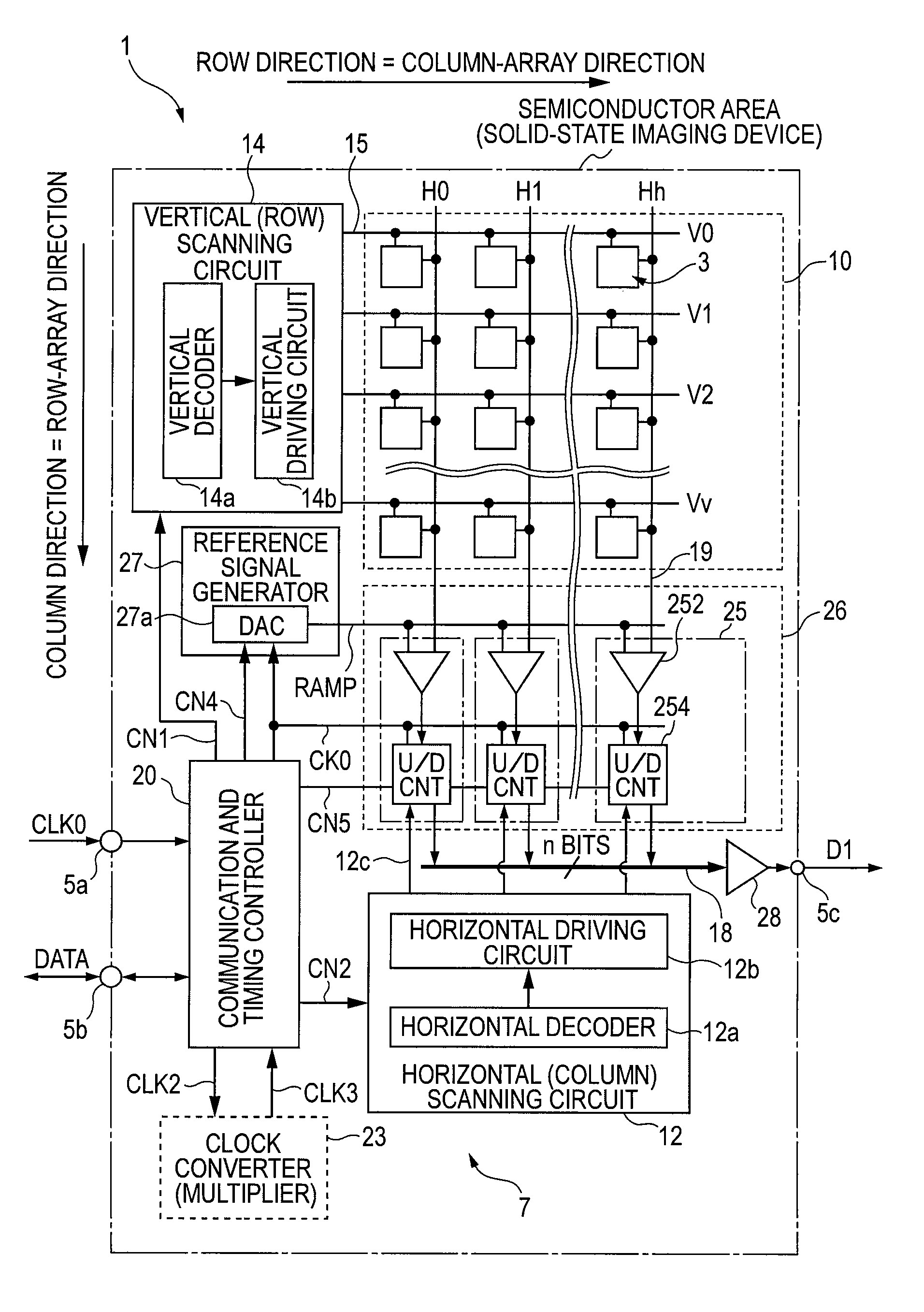
[0114]FIG. 1 is a schematic configuration diagram of a CMOS solid-state imaging device (CMOS image sensor) 1 as an implementation of a semiconductor device according to a first embodiment of the present invention. The CMOS solid-state imaging device 1 is also an implementation of an electronic apparatus according to an embodiment of the present invention.

[0115] The solid-state imaging device 1 includes a pixel unit 10 having a plurality of pixels 3 arranged in rows and columns (or in a two-dimensional matrix). Each of the pixels 3 includes a photosensitive element (which is one example of charge generator) that outputs a voltage signal corresponding to the amount of incident light. In the solid-state imaging device 1, correlated double sampling (CDS) processors and analog-to-digital converters (ADCs) are provided in a column-parallel manner.

[0116] More specifically, a plurality of CDS processors and ADCs are provided substantially in parallel to vertical signal lines 19 of columns...

second embodiment

[0199]FIG. 3 is a schematic configuration diagram of a CMOS solid-state imaging device (CMOS image sensor) 1 according to a second embodiment of the present invention. In the solid-state imaging device 1 according to the second embodiment, each of the column A / D circuits 25 according to the first embodiment is modified.

[0200] Each of column A / D circuits 25 according to the second embodiment includes a counter 254, a data storage unit 256 serves as an n-bit memory, and a switch 258. The data storage unit 256 is placed downstream of the counter 254, and stores a count value stored in the counter 254. The switch 258 is placed between the counter 254 and the data storage unit 256.

[0201] A memory-transfer instruction pulse CN8 is commonly supplied as a control pulse at a predetermined timing from the communication and timing controller 20 to the switches 258 provided for the respective columns. In response to the memory-transfer instruction pulse CN8, each of the switches 258 transfers...

third embodiment

[0210]FIG. 5 is a schematic circuit diagram of a voltage comparator 252 used in a CMOS solid-state imaging device (CMOS image sensor) 1 according to a third embodiment of the present invention. In the solid-state imaging device 1 according to the third embodiment, the voltage comparator 252 in the solid-state imaging device 1 according to the first embodiment is modified so that the comparison period can be set irrespective of variations in the reset component .DELTA.V. The details will now be described.

[0211] The voltage comparator 252 shown in FIG. 5 has a known differential amplifier configuration, as in the comparator disclosed in the fifth non-patent document noted above (see FIG. 8). The voltage comparator 252 includes a differential transistor pair 300 having NMOS transistors 302 and 304, a load transistor pair 310 having a p-channel MOS (PMOS) transistors 312 and 314, and a current source 320 having an NMOS constant-current source transistor 322. The load transistor pair 31...


PUM


Abstract

In an analog-to-digital conversion method for converting a difference signal component representing a difference between a reference component and a signal component in an analog signal to be processed into digital data, in a first process, a signal corresponding to one of the reference component and the signal component is compared with a reference signal for conversion into the digital data. Concurrently with the comparison, counting is performed in one of a down-count mode and an up-count mode, and a count value at a time of completion of the comparison is held. In a second process, a signal corresponding to the other one of the reference component and the signal component is compared with the reference signal. Concurrently with the comparison, counting is performed in the other one of the down-count mode and the up-count mode, and a count value at a time of completion of the comparison is held.

Description

CROSS REFERENCES TO RELATED APPLICATIONS [0001] The application is a continuation application of the U.S. patent application Ser. No. 11 / 268,428, filed in the United States Patent and Trademark Office on Nov. 7, 2005, the entire contents of which are incorporated herein by reference to the extent permissible by law. This application claims the benefit priority of Japanese Priority document JP 2004-323432, filed in the Japanese Patent Office on Nov. 8, 2004, the entire contents of which are incorporated herein by reference to the extent permissible by law.BACKGROUND OF THE INVENTION [0002] 1. Field of the Invention [0003] The present invention relates to an analog-to-digital (A / D) conversion method, and an A / D converter, a semiconductor device having a plurality of unit elements for detecting distribution of a physical quantity, and an electronic apparatus. More specifically, the present invention relates to a technique for converting analog output electrical signals into digital dat...

Claims


Application Information

Patent Timeline
Patent Type & Authority Applications(United States)
IPC IPC(8): H03M1/06H04N5/378
CPCH03K5/2481H03K5/249H03M1/1023H04N5/378H03M1/1295H03M1/56H03M1/123H04N25/75H03M1/12H04N23/00
Inventor MURAMATSU, YOSHINORIFUKUSHIMA, NORIYUKINITTA, YOSHIKAZUYASUI, YUKIHIRO
Owner SONY CORP
Why Eureka
Try Eureka