White electroluminescent device and method of producing the same

a technology of electroluminescent devices and white electroluminescent devices, which is applied in the direction of discharge tube luminescent screens, energy-saving lighting, sustainable buildings, etc., to achieve the effects of enhancing white color purity and luminescent efficiency, and improving white luminescent efficiency

Inactive Publication Date: 2007-02-15
SAMSUNG MOBILE DISPLAY CO LTD
View PDF23 Cites 36 Cited by
  • Summary
  • Abstract
  • Description
  • Claims
  • Application Information

AI Technical Summary

Benefits of technology

[0009] It is therefore a feature of an embodiment of the present invention to provide a white EL device that provides pure white color coordinates and improved white luminescent efficiency.
[0010] It is another feature of an embodiment of the present invention to provide a method of producing a white EL device having an improved structure providing enhanced white color purity and luminescent efficiency.

Problems solved by technology

However, a multi-layered structure of light emitting layers between two electrodes in a white EL device may trigger a resonance effect that may modify the displayed white light.

Method used


Image

  • White electroluminescent device and method of producing the same
  • White electroluminescent device and method of producing the same
  • White electroluminescent device and method of producing the same

Examples


example 1

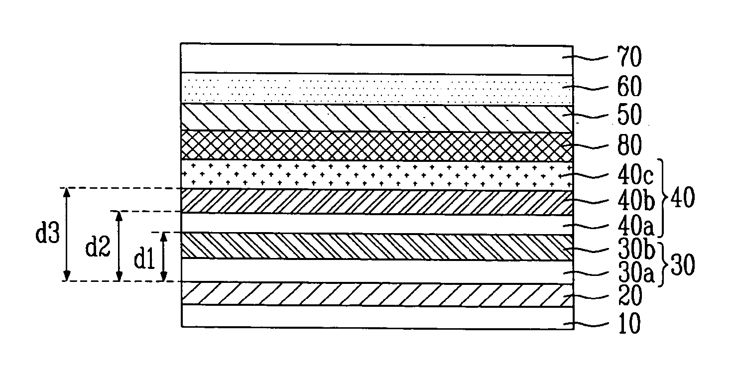
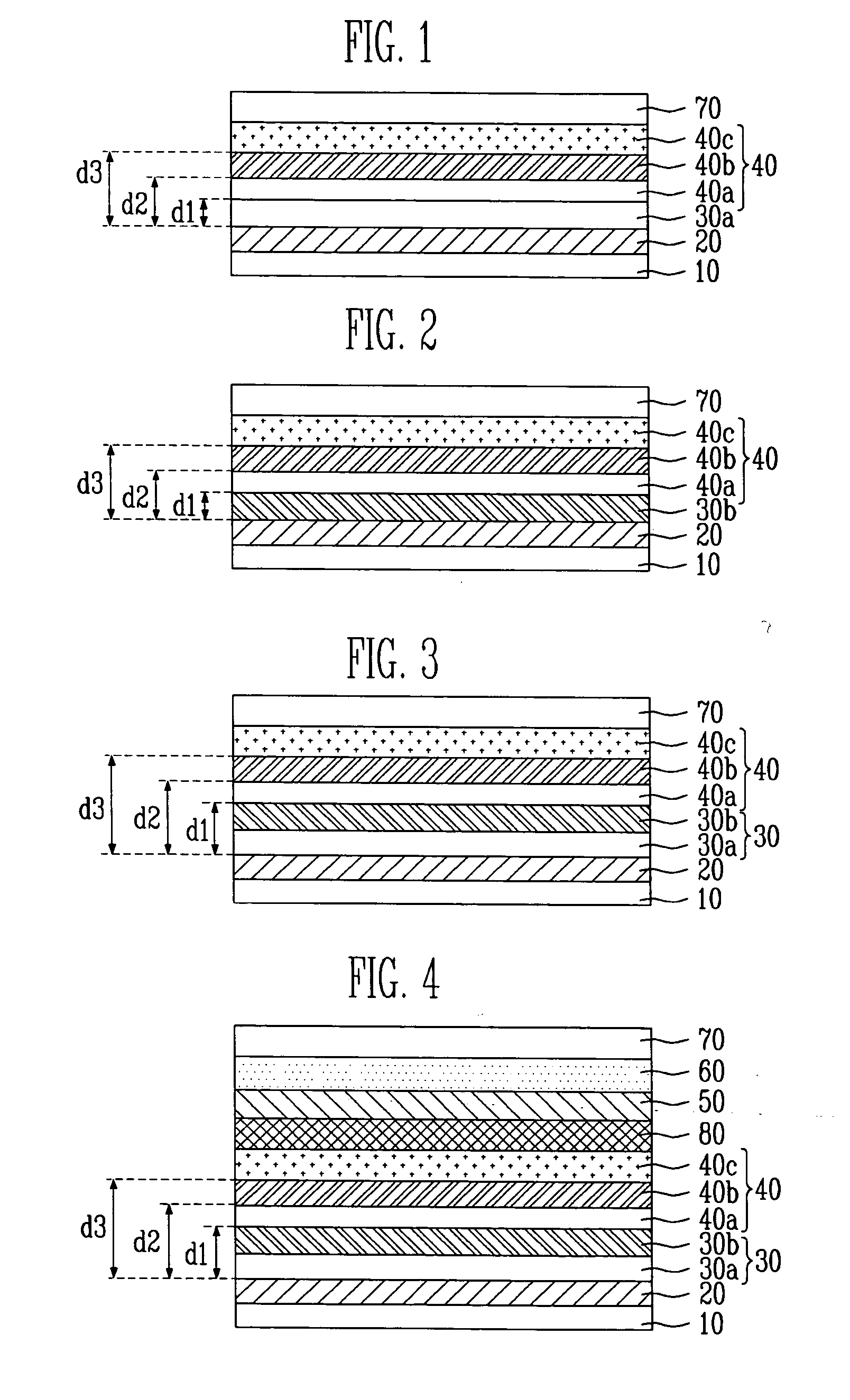
[0062] A white EL device according to an embodiment of the present invention was prepared as follows. A glass substrate was obtained and an ITO layer having a thickness of 10 nm was electrodeposited thereon to form an anode. A layer of Ag having a thickness of 100 nm was deposited on top of the anode to form a reflective film, thereby forming a reflective electrode. Next, a layer of NPD having a thickness of 15 nm was deposited on the upper surface of the first electrode under a vacuum pressure of 10−6 torr to form a hole transporting layer.

[0063] A layer of DPVBI was deposited on the upper surface of the hole transporting layer to form a blue emitting layer having a thickness of 15 nm. Next, Alq3 was deposited on top of the blue emitting layer to form a green emitting layer having a thickness of 20 nm, and rubrene was deposited on top of the green emitting layer to form a red emitting layer having a thickness of 40 nm. Subsequently, an electron transporting material Alq3 was depos...

example 2

[0064] The white EL device of Example 1 was prepared, except that the hole transporting layer was formed to have a thickness of 15 nm, and the blue, green, and red emitting layers were formed to have thickness values of 25 nm, 20 nm, and 40 nm, respectively.

example 3

[0065] A white EL device according to another embodiment of the present invention was prepared as follows. A glass substrate was obtained and an ITO layer having a thickness of 10 nm was electrodeposited thereon to form an anode. A layer of Ag having a thickness of 100 nm was deposited on top of the anode to form a reflective film, thereby forming a reflective electrode. Next, a layer of IDE406 (commercially available from the company Idemitsu) was deposited on the upper surface of the first electrode to form a hole injection layer having a thickness of 150 nm, and a layer of NPD was deposited thereon to form a hole transporting layer having a thickness of 10 nm. Both depositions were performed under vacuum pressure conditions of 10−6 torr.

[0066] A layer of DPVBI was used on top of the hole transporting layer to form a blue emitting layer having a thickness of 30 nm, Alq3:C545T was used to form a green emitting layer having a thickness of about 20 nm, and Alq3:DCJTB was used to for...


PUM


Abstract

A white electroluminescent (EL) device and a method of preparing the same, includes a substrate, a first electrode, a hole transporting unit having a predetermined transporting unit thickness, a blue emitting layer having a predetermined blue layer thickness, a green emitting layer having a predetermined green layer thickness, a red emitting layer, and a second electrode, wherein the white EL device is capable of displaying white light having color coordinates of from about (0.27, 0.27) to about (0.39, 0.39).

Description

BACKGROUND OF THE INVENTION [0001] 1. Field of the Invention [0002] The present invention relates to a white electroluminescent device and a method of producing the same. More particularly, the present invention relates to a white electroluminescent device and a method of producing the same, wherein the white electroluminescent device has a novel structure providing improved color purity and white luminescent efficiency. [0003] 2. Discussion of the Related Art [0004] Generally, an electroluminescent (EL) device is a display device wherein voltage may be employed in light emitting layers to combine electrons and holes. The combination of electrons and holes may excite electrons in light emitting layers and, thereby, cause the light emitting layers to emit photons in the form of visible light to form images. EL devices have superior characteristics as compared to other display devices, such as excellent visibility, light weight, reduced thickness, and relatively low power consumption....

Claims


Application Information

Patent Timeline
Patent Type & Authority Applications(United States)
IPC IPC(8): H01J1/62H01J63/04
CPCC09K11/06C09K2211/1007C09K2211/1011C09K2211/1029Y02B20/181C09K2211/1088H01L51/5036H01L2251/558H05B33/14C09K2211/1037Y02B20/00H10K50/125H10K2102/351H05B33/10
Inventor LEE, JUN YEOB
Owner SAMSUNG MOBILE DISPLAY CO LTD
Why Eureka
Try Eureka