3D IC method and device
a three-dimensional integrated circuit and integrated circuit technology, applied in the field of three-dimensional integrated circuit devices and the fabrication thereof, can solve the problems of increasing ic cost, reducing chip yield, and reducing yield
- Summary
- Abstract
- Description
- Claims
- Application Information
AI Technical Summary
Problems solved by technology
Method used
Image
Examples
first embodiment
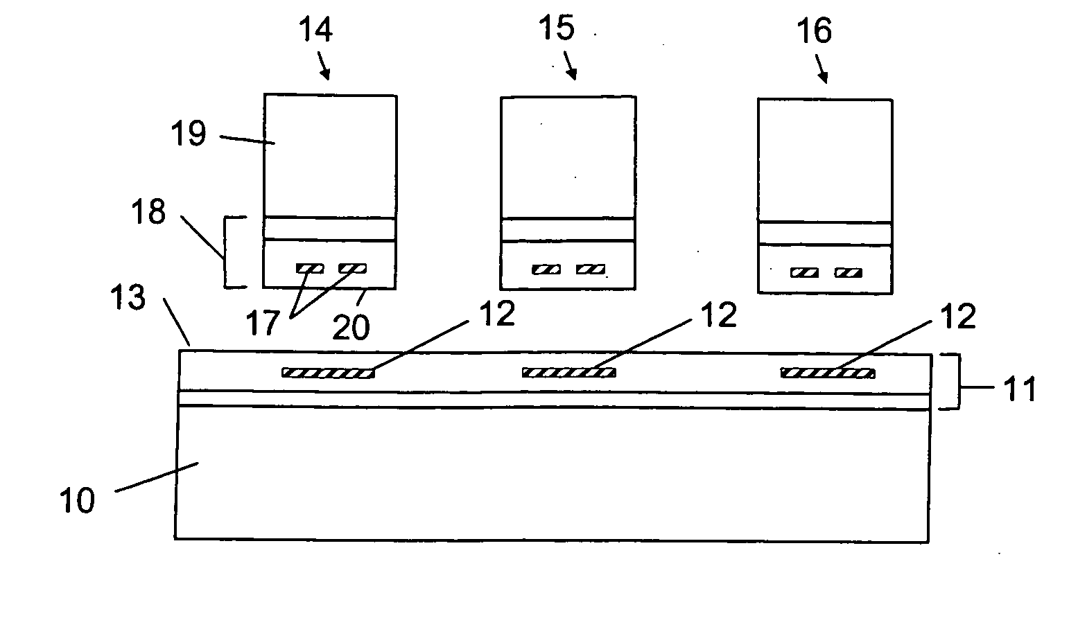
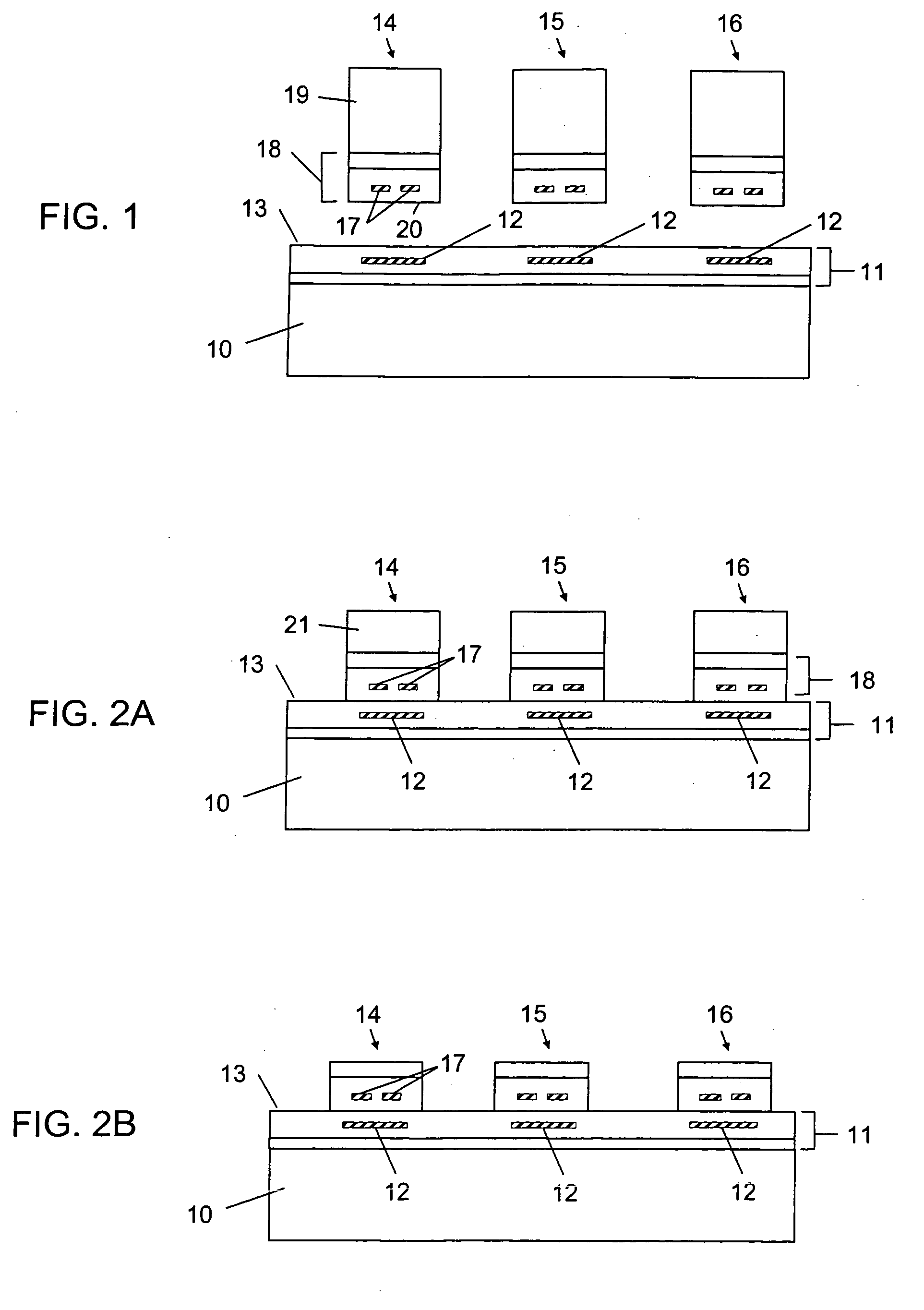
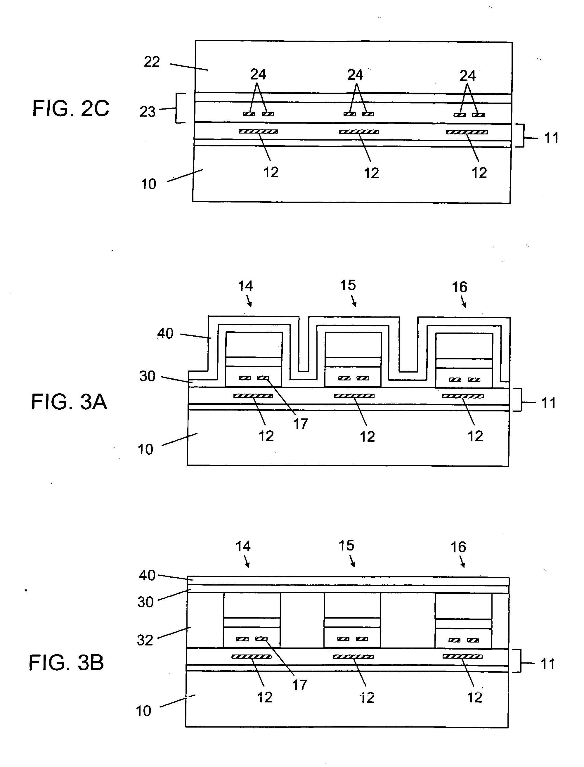
[0063] Referring now to the drawings, in particular FIG. 1, the method according to the invention will be described. It is noted here that the drawings are not drawn to scale but are drawn to illustrate the concepts of the invention.
[0064] Substrate 10 includes a device region 11 having contact structures 12. Substrate 10 may be made of a number of materials, such as semiconductor material or insulating material, depending on the desired application. Typically, substrate 10 is made of silicon or III-V materials. Contact structures 12 are typically metal pads or interconnect structures making contact to device or circuit structures (not shown) formed in substrate 10. Substrate 10 may also contain an integrated circuit to which the contact structures 12 are connected, and substrate 10 may be a module containing only contact structures. For example, substrate 10 may be a module for interconnecting structures bonded to substrate 10, or bringing out connections for packaging or integrati...
fourth embodiment
[0066] Die 14-16 may be of the same technology as wafer 10, or of different technology. Die 14-16 may each be the same or different devices or materials. Each of die 14-16 has conductive structures 17 formed in a device region 18. Structures 17 are spaced apart to leave a gap therebetween, or may be a single structure with an aperture which may extend across the entire contact structure. In other words, the aperture may be a hole in contact structure or may divide the contact structure in two. The size of the gap or aperture may be determined by the photolithographic design rules for the particular technology being bonded. For example, a minimum lateral width of contact structures 12 and 17 may be required to subsequently form a reliable, low resistance electrical connection with interconnect metal An additional factor that determines the optimum size of the gap or aperture is a ratio of a distance given by the vertical separation between contact structures 17 and 12 plus the thickn...
fifth embodiment
[0112] A fifth embodiment is shown in FIGS. 20A-20H. This embodiment is similar to the previous embodiments before the formation of via 50 with the exception that contact structures in die 17, 108, 117, or 123 with an aperture or edge that overlaps via 50 is replaced with contact structure 87 without an aperture or overlapping edge. In this embodiment, contact structures 87 in die 84-86 with substrate portion 89, device region 88 are bonded to surface 83 with device region 81, substrate 80, and contact structures 82. Contact structure 87 is positioned over contact structure 82 as shown in FIG. 20A. Die 84-86 can also be bonded to a surface 113 with exposed contact structures 112 similar to that shown in FIGS. 16 and 17 or contact structures 122 similar to that shown in FIGS. 18 and 19. Note that the contact structure 87 may be bonded in direct contact with contact structure 82, which is illustrated in device 86. Dies 84-86 may also have the same contact structure configuration. FIGS...
PUM
 Abstract
Description
Claims
Application Information


