

Nitride-based semiconductor device and method of manufacturing the same
a technology of nitride and semiconductors, applied in the field of semiconductor devices, can solve the problems of difficult fabrication, good yield, distortion of barrier layer,
- Summary
- Abstract
- Description
- Claims
- Application Information
AI Technical Summary
Benefits of technology
Problems solved by technology
Method used
Image

Examples
Embodiment Construction
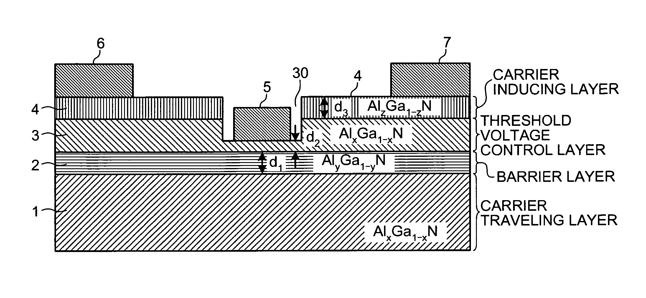
[0039] Preferred embodiments of a nitride-based semiconductor device and a method of manufacturing the same according to the present invention will be explained in detail with reference to the appended drawings. The present invention is not limited to the embodiments. Further, the sectional view of the nitride-based semiconductor device used in the following embodiments are schematic, and the relationship between the thickness and width of the layer and the ratio of the thickness of each layer are different from those of a real device.
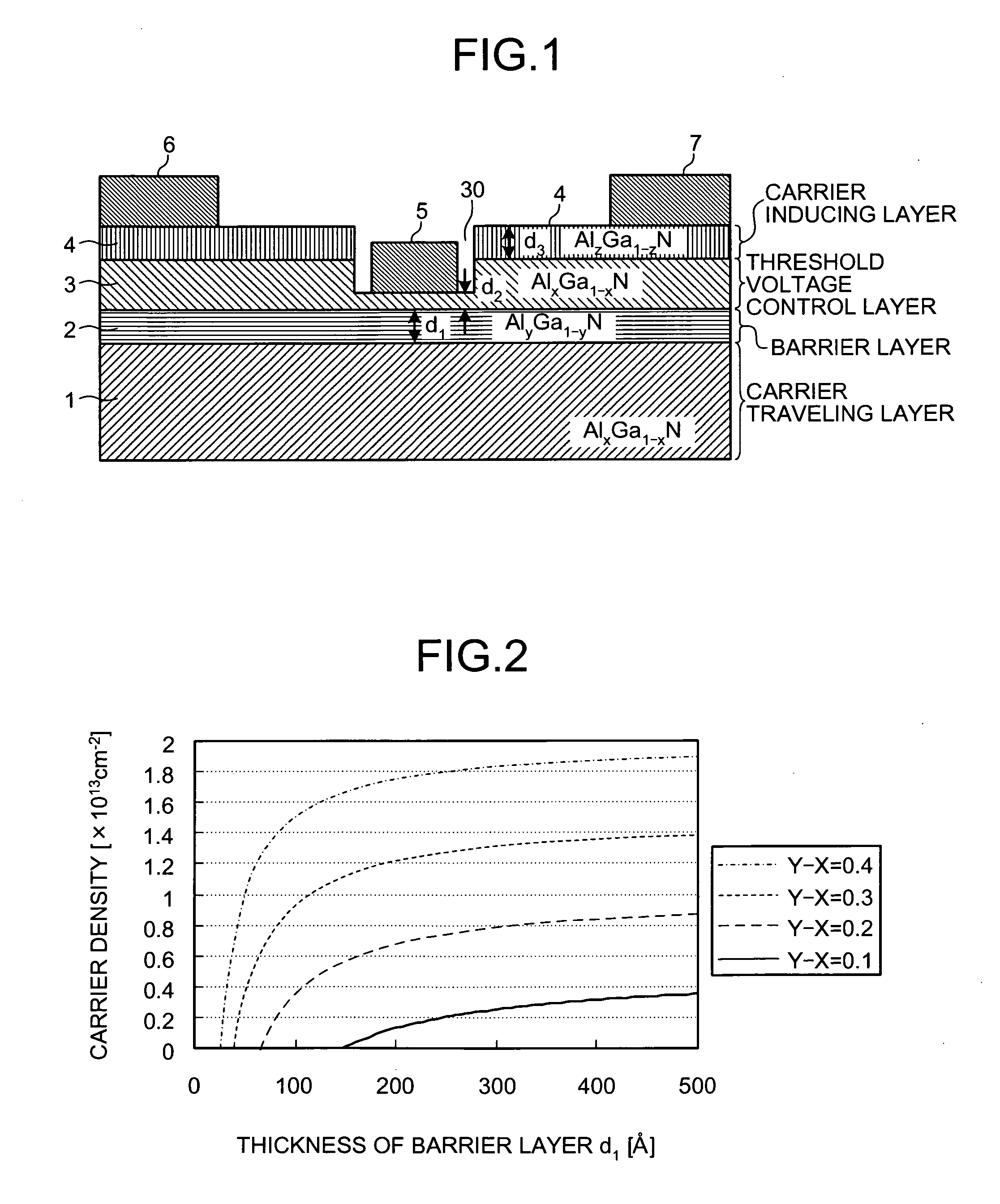
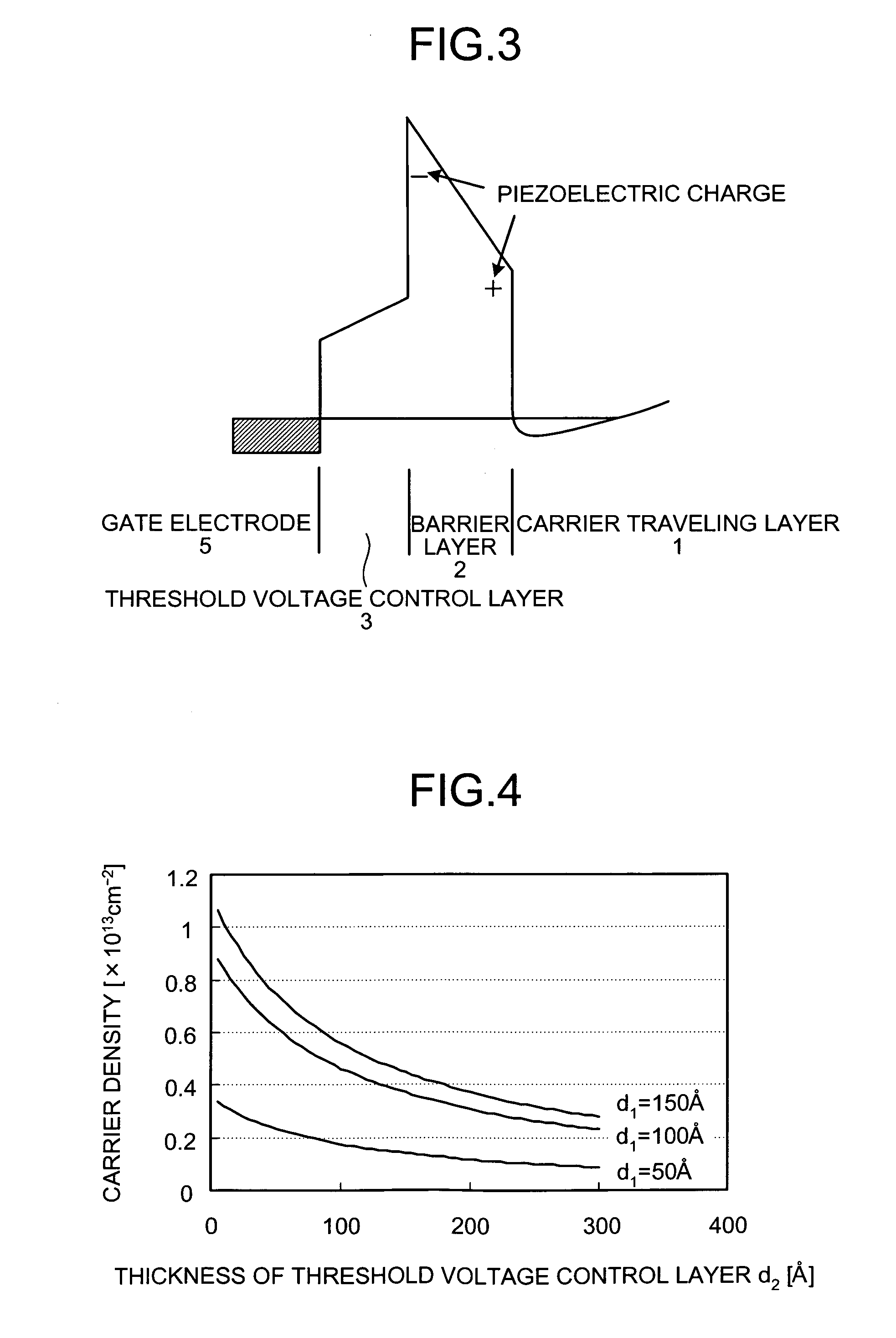
[0040]FIG. 1 is a sectional view schematically showing a configuration of a nitride-based semiconductor device according to this embodiment. This nitride-based semiconductor device has a configuration in which a carrier traveling layer 1 composed of AlxGa1-xN (0≦X2 composed of AlYGa1-YN ((01, a threshold voltage control layer 3 composed of a non-doped semiconductor having a lattice constant equal to that of the carrier traveling layer 1, and a carrier...
PUM
 Abstract
Description
Claims
Application Information