Radio frequency identification tag and manufacturing method thereof

a technology of radio frequency identification and manufacturing method, which is applied in the field of radio frequency identification tags, can solve the problems of increasing the size and cost of the package, and not being suitable for packaging medicines in general, and achieves the effect of long communication distan

Inactive Publication Date: 2007-03-01
HITACHI LTD
View PDF5 Cites 29 Cited by
  • Summary
  • Abstract
  • Description
  • Claims
  • Application Information

AI Technical Summary

Benefits of technology

[0008] According to this invention, an inlet is prepared in which an IC chip is mounted on a small antenna formed with an impedance matching circuit. This inlet is mounted on an antenna implemented by a slot or an island area formed on an aluminum sheet of a package thereby to realize a “RFID tag”. As a result, the inlet itself can function as a small “RFID tag” on the one hand, and the radio wave is amplified by the operation of the antenna formed on the aluminum sheet on the other hand. Even a “RFID tag” mounted on the metal surface, therefore, can radiate a strong radio wave. Thus, a “RFID tag” mounted on the aluminum sheet package can secure a long communication distance.

Problems solved by technology

The use of a “RFID tag” suitable for a metal, however, would increase the size and cost of the package and therefore not suitable for packaging medicines in general.

Method used


Image

  • Radio frequency identification tag and manufacturing method thereof
  • Radio frequency identification tag and manufacturing method thereof
  • Radio frequency identification tag and manufacturing method thereof

Examples


first embodiment

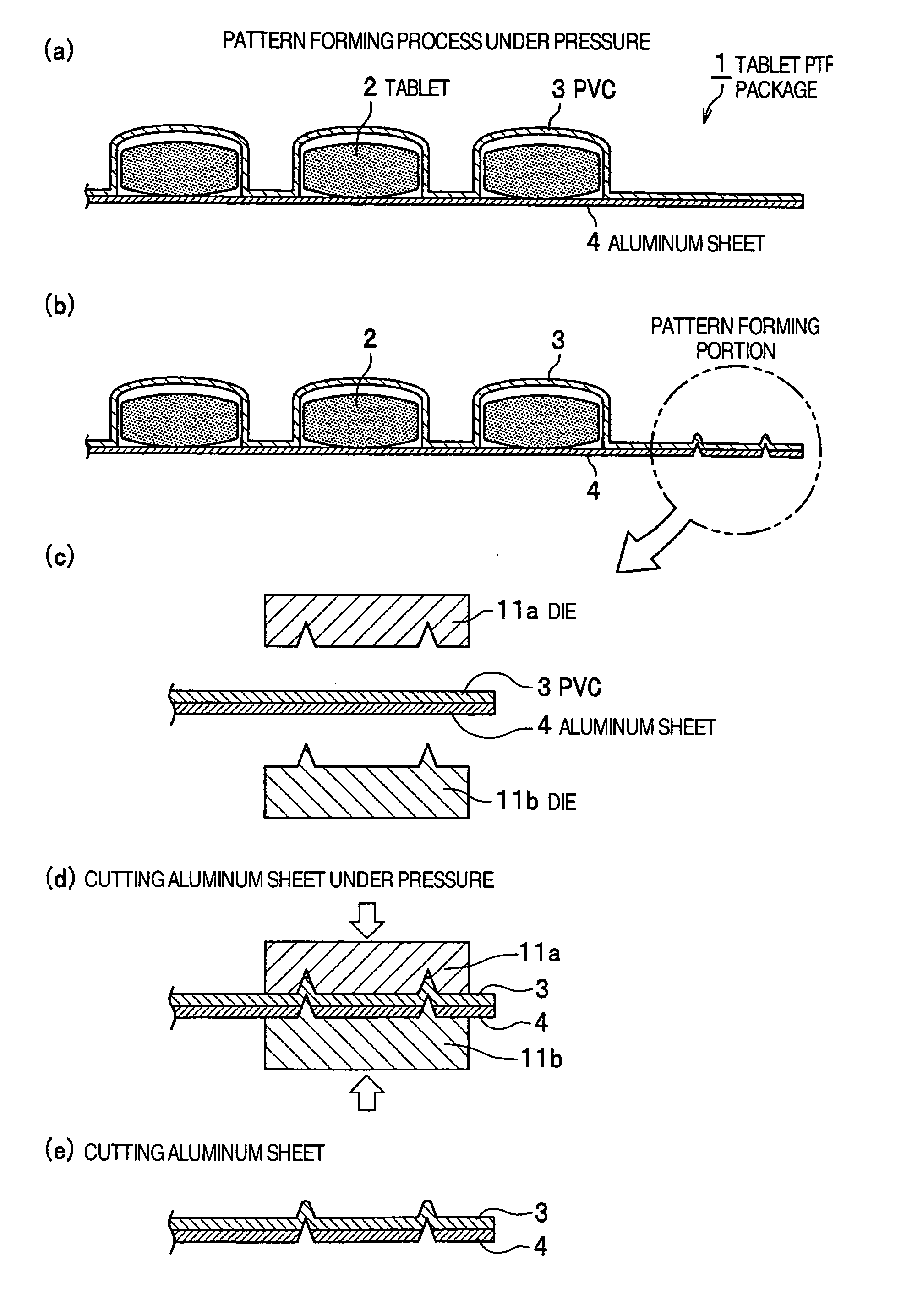
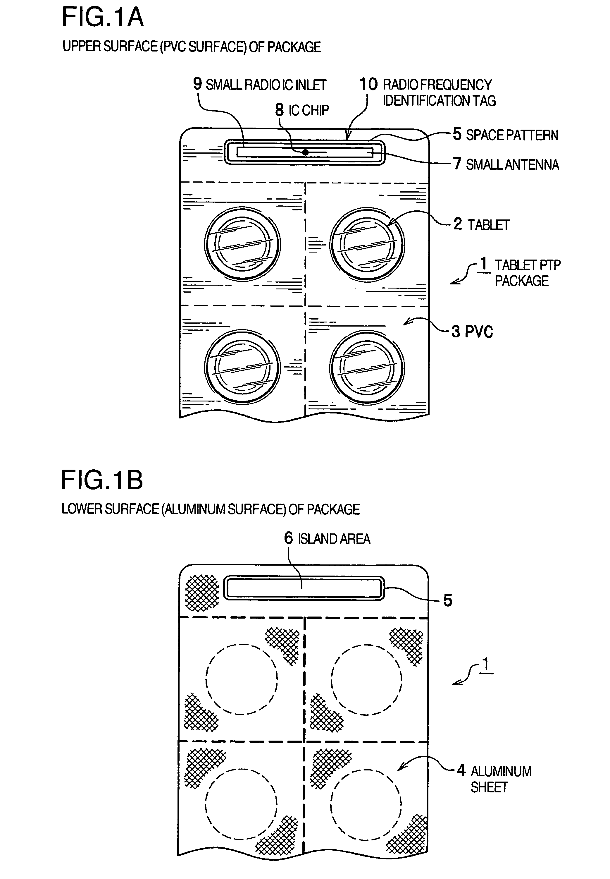
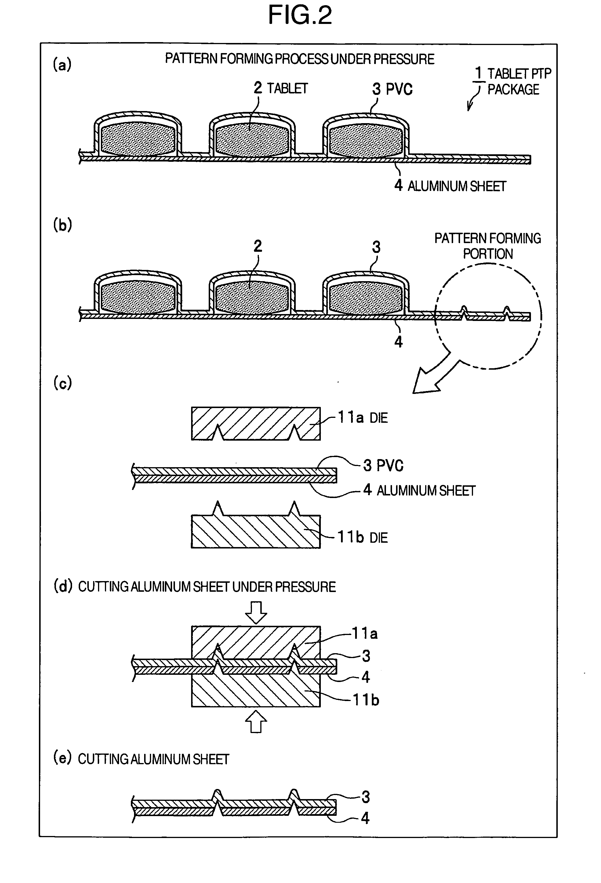
[0029]FIGS. 1A and 1B show the appearance of the tablet PTP package with the “RFID tag” mounted thereon. FIG. 1A shows the upper surface (PVC surface) of the package, and FIG. 1B the lower surface (aluminum surface) thereof. As shown in FIGS. 1A and 1B, the tablet PTP package 1 includes a multiplicity of tablets 2 packed by a PVC 3 and an aluminum sheet 4. As shown in FIG. 1B, an elongate space pattern 5 is formed in a part (upper part, for example) of the aluminum sheet 4 on the lower surface of the package thereby to form an island area 6 constituting an antenna area. Also, as shown in FIG. 1A, a small radio IC inlet 9 with an IC chip 8 mounted on a small antenna 7 is arranged on the reverse surface of the portion of the aluminum sheet 4 (i.e. the upper surface of the package) formed with the island area 6. Specifically, the small radio IC inlet 9, as shown in FIG. 1A, is arranged on the surface of the PVC 3 on the upper surface of the package.

[0030] The antenna area and the smal...

second embodiment

[0035] As a second embodiment of the invention, variations of the space pattern forming an island area or a peninsular area are explained. FIG. 4 is a diagram showing variations of the space pattern of an island area or a peninsular area formed on the aluminum sheet of the tablet PTP package according to the second embodiment of the invention. The basic form of (a) in FIG. 4 is a first variation of the space pattern forming an island area for linear polarization (unidirectional polarization) with the wavelength of λ / 2. A first modification shown in (b) of FIG. 4 is a second variation of the space pattern forming a U-shaped peninsular area linear polarization (unidirectional polarization) with the wavelength of λ / 4.

[0036] With the peninsular pattern as the first modification shown in (b) of FIG. 4, for example, the “RFID tag” can be formed one half in size of the basic form shown in (a) of FIG. 4. Thus, the “RFID tag” can be mounted on a still smaller PTP package and the application...

third embodiment

[0044] As a third embodiment, several variations in which a slotted space pattern is formed in a wide metal foil area are explained. FIG. 5 is a diagram showing variations in which a slotted space pattern is formed in a wide metal foil area according to the third embodiment of the invention. In (a) of FIG. 5, a basic form is shown in which a linear slotted space pattern of λ / 2 long is formed in the metal foil area for linear polarization with the wavelength of λ / 2. The first modification shown in (b) of FIG. 5 represents a modification of the basic form shown in (a) of FIG. 5 and represents a state in which the linear slotted space pattern λ / 4 long is formed in the metal foil area for linear polarization with the wavelength of λ / 4.

[0045] The second modification shown in (c) of FIG. 5 derives from the basic form shown in (a) of FIG. 5, and represents the state in which a hook-shaped slotted space pattern is formed in the metal foil area from a linear pattern λ / 2 long for bidirection...


PUM


Abstract

A tablet PTP package contains a multiplicity of tablets by a resin PVC and a metal sheet such as an aluminum sheet. An elongate space pattern is formed in a part of the aluminum sheet on the lower surface of the package to form an island area constituting an antenna. A small radio IC inlet including an IC chip mounted on a small antenna is arranged on the reverse surface (upper surface of the package) of the portion of the aluminum sheet corresponding to the island area. The small radio IC inlet and the second antenna formed by the island area are electrostatically coupled to each other with the resin PVC as a dielectric member, and thus a RFID (radio frequency identification) tag is configured.

Description

BACKGROUND OF THE INVENTION [0001] This invention relates to a radio frequency identification tag (RFID tag) for transmitting the information recorded in an IC chip by radio communication, or in particular to a “RFID tag” mounted on the surface of a metal sheet and a “RFID tag” manufacturing method. [0002] In recent years, a “RFID tag” has come to find wide applications for information control of articles and structures or distribution control. The “RFID tag” is configured of a small IC chip having recorded information therein and a small antenna for transmitting the information in the IC chip by radio communication. The “RFID tag” is used by being attached to an article or buried in a structure. The IC chip is as small as about 0.4 mm×0.4 mm size by 0.1 mm high. By bringing a reader-writer in proximity to this “RFID tag”, the information (i.e. the information on the attributes of individual articles and structures) recorded in the IC chip can be read without contact. Considering th...

Claims


Application Information

Patent Timeline
Patent Type & Authority Applications(United States)
IPC IPC(8): G08B13/14G16H20/13
CPCA61J1/035A61J2205/60H01Q9/0407H01Q1/22H01Q1/2225G06K19/07756G16H20/13
Inventor SAKAMA, ISAOASHIZAWA, MINORU
Owner HITACHI LTD
Why Eureka
Try Eureka