High-performance memory and related method
- Summary
- Abstract
- Description
- Claims
- Application Information
AI Technical Summary
Benefits of technology
Problems solved by technology
Method used
Image
Examples
Embodiment Construction
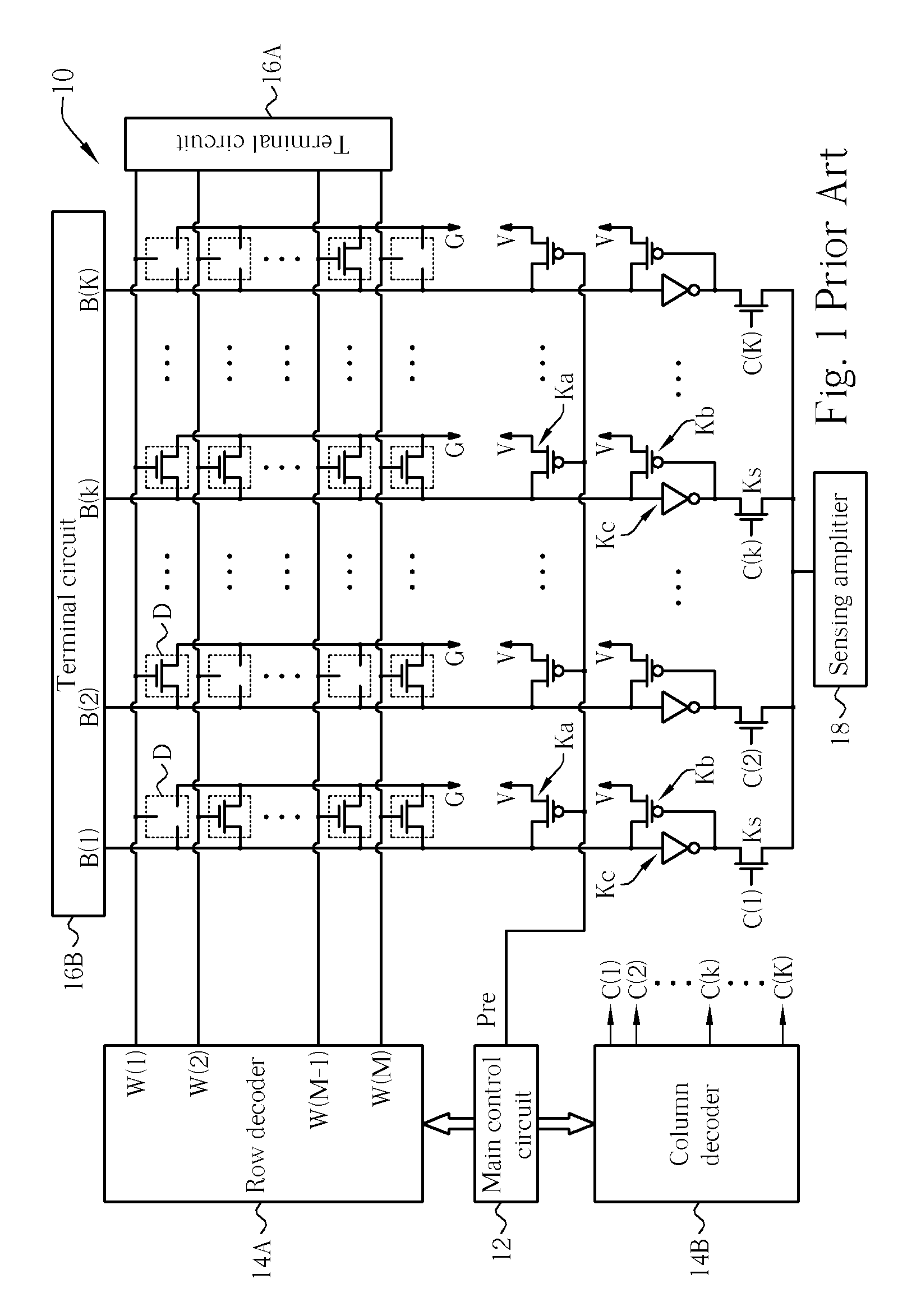
[0020]FIG. 1 is a diagram of a conventional memory circuit 10. The memory units are arranged in array, each memory unit D has a corresponding row line and column line respectively which represents one bit of data. The memory units are arranged in array by intersecting the row lines (or the word lines) W(1), . . ., W(M) and the column lines (or the bit lines) B(1), . . ., B(K). The memory circuit 10 further includes a mastering circuit 12, a column decoder 14B, a row decoder 14A, two terminal circuits 16A and 16B, and a sense amplifier 18. In addition, each of column line has two p-type metal oxide semiconductors Ka and Kb, an inverter Kc, and an N-type metal oxide semiconductor Ks utilized as a switch. The memory circuit 10 is biased between a high voltage V (e.g. a positive voltage VDD), and a low voltage G (e.g. a ground voltage). The mastering circuit 12 controls the operations of the memory circuit 10 and provides a pre-charging signal Pre to control pre-charging timing. Both th...
PUM
 Abstract
Description
Claims
Application Information


