
High-performance memory and related method

a high-performance memory and memory technology, applied in the field of memory, can solve the problems of large power consumption, memory units spending much more time on discharging, and conventional memory, and achieve the effect of enhancing the increment of voltag

Active Publication Date: 2008-01-10
VIA TECH INC
View PDF4 Cites 0 Cited by
  • Summary
  • Abstract
  • Description
  • Claims
  • Application Information

AI Technical Summary

Benefits of technology

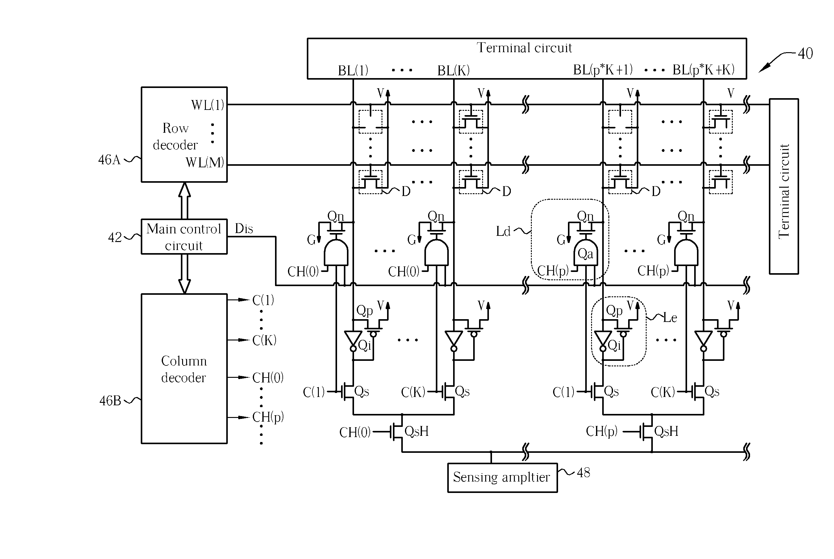
The present invention provides a memory circuit and a method for accessing a memory. The memory circuit includes a discharging module, an auxiliary module, and a sense amplifier. The discharging module discharges the column line of an objective memory unit, the auxiliary module enhances the increment of the voltage level of the column line, and the sense amplifier accesses data stored in the memory unit by detecting an electrical level of the column line. The method includes decoding and discharging the column line of an objective memory unit, decoding the column line of the objective memory unit and enabling the memory unit through the column line to change the voltage level of the column line of the objective memory unit, accessing the objective memory unit according to the voltage level of the column line, and turning on a driving unit for enhancing the increment of the voltage when the voltage level of the column line reaches a threshold voltage level. The technical effects of the invention include improving the speed and accuracy of accessing data stored in the memory, and reducing the power consumption of the memory circuit.

Problems solved by technology

However, the conventional memory has some disadvantages.
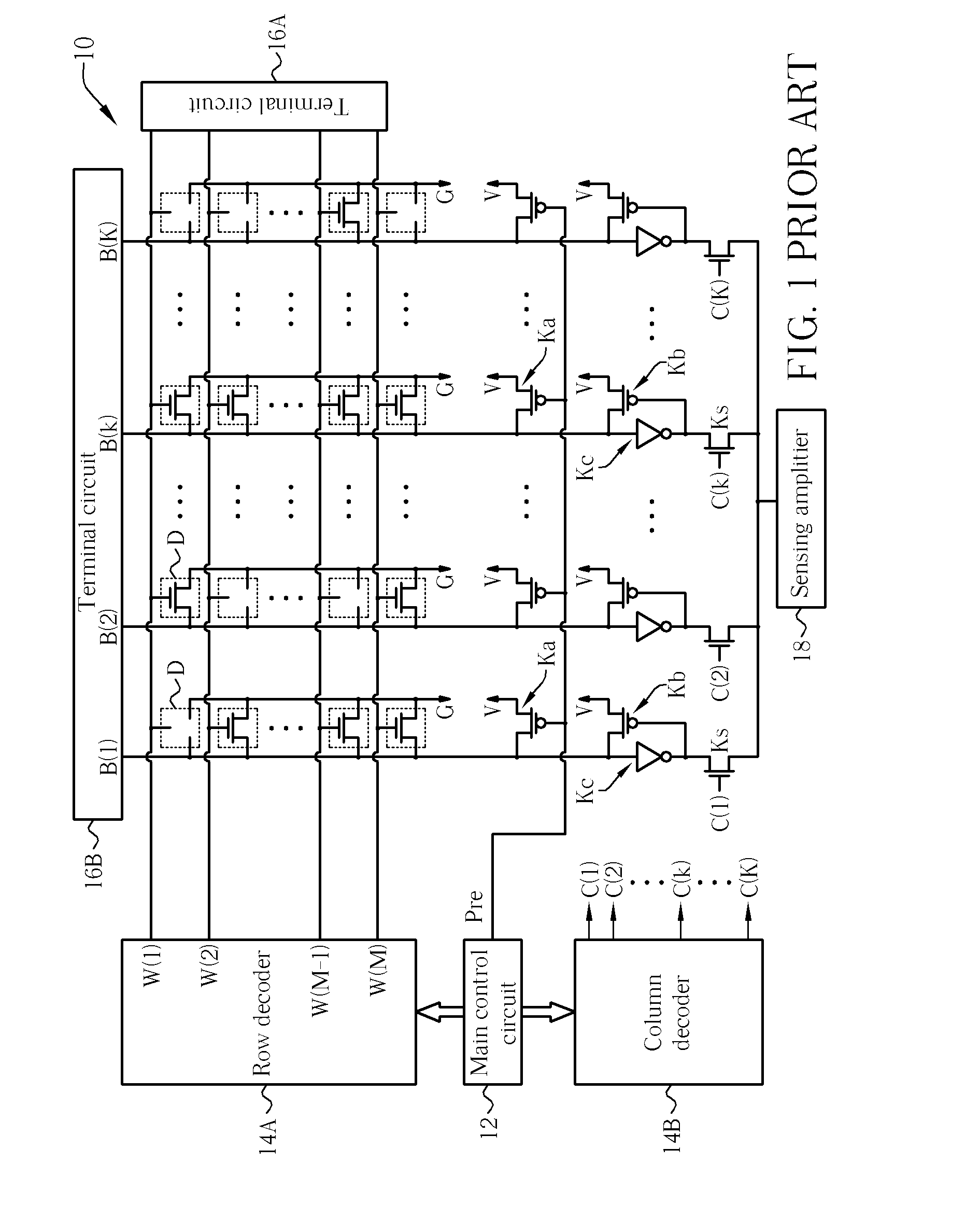
When accessing an objective memory unit, the conventional memory has to pre-charge all of the column lines, so that a great power is consumed.
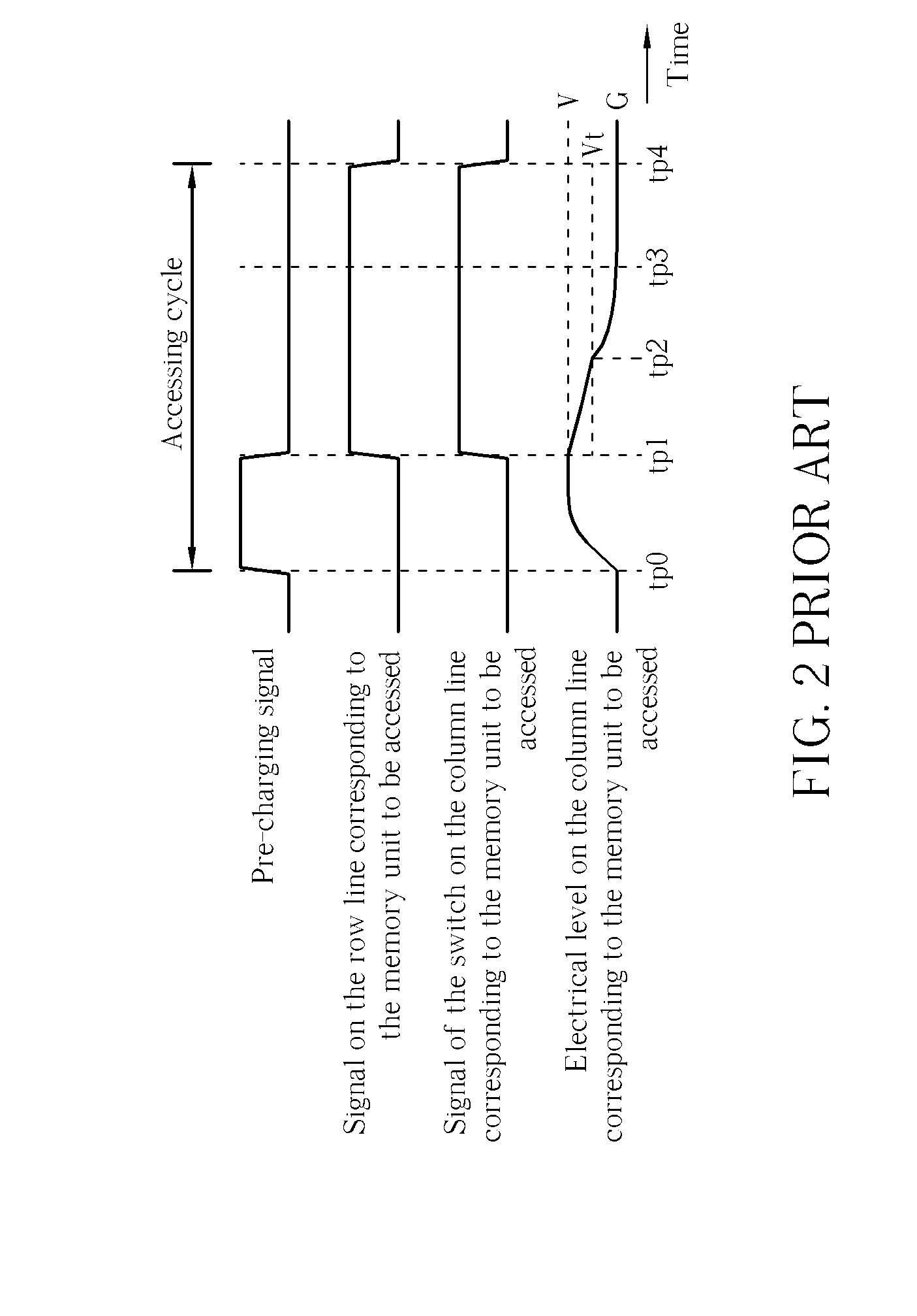
Unfortunately, for maintaining the voltage level of the column line, the holding circuit must fight against the discharging of the memory unit, and thus, the memory unit spends much more time on discharging.
In other words, the accessing cycle of the conventional memory is relatively long, which results in a low accessing efficiency.

Method used


Image

  • High-performance memory and related method
  • High-performance memory and related method
  • High-performance memory and related method

Examples


Embodiment Construction

[0019]FIG. 1 is a diagram of a conventional memory circuit 10. The memory units are arranged in array, each memory unit D has a corresponding row line and column line respectively which represents one bit of data. The memory units are arranged in array by intersecting the row lines (or the word lines) W(1), . . . , W(M) and the column lines (or the bit lines) B(1), . . . , B(K). The memory circuit 10 further includes a mastering circuit 12, a column decoder 14B, a row decoder 14A, two terminal circuits 16A and 16B, and a sense amplifier 18. In addition, each of column line has two p-type metal oxide semiconductors Ka and Kb, an inverter Kc, and an N-type metal oxide semiconductor Ks utilized as a switch. The memory circuit 10 is biased between a high voltage V (e.g. a positive voltage VDD), and a low voltage G (e.g. a ground voltage). The mastering circuit 12 controls the operations of the memory circuit 10 and provides a pre-charging signal Pre to control pre-charging timing. Both ...


PUM


Abstract

In memory array of a memory circuit, a discharging module and an auxiliary module are disposed on each column line. While accessing an objective memory unit on a column line of the memory, the memory unit discharges the corresponding row line of the objective memory unit according to a discharging signal and a column selective signal. When the objective memory unit is enabled, the voltage level of the corresponding column line is changed, if the voltage level reaches a threshold voltage level, the auxiliary module enhances the increment of the voltage level of the column line.

Description

CROSS REFERENCE TO RELATED APPLICATIONS [0001] This application is a division of U.S. application Ser. No. 11 / 463,890 filed Aug. 10, 2006, the entirety of which is included herein by reference.BACKGROUND OF THE INVENTION [0002] 1. Field of the Invention [0003] The present invention relates to the field of memories, and more particularly, to a memory and a related method capable of decreasing power consumption and enhancing accessing efficiency. [0004] 2. Description of the Prior Art [0005] In modern information society, documents and data are transmitted, managed, and stored in the form of electronic signals, for this reason, memory device and memory circuits capable of accessing data are widely used in various fields. For example, in the field of communication, read-only memories, which store data in a non-volatile manner, generally are disposed in communication chips of cell phones for storing codes utilized for processing signals or other necessary parameters and vectors. [0006] ...

Claims


Application Information

Patent Timeline
Patent Type & Authority Applications(United States)
IPC IPC(8): G11C7/12
CPCG11C7/12
Inventor CHENG, CHI-TING
Owner VIA TECH INC
Learn More