Flash memory with recessed floating gate

a floating gate and flash memory technology, applied in the field of flash memory devices with recessed floating gate structures, can solve the problems of reducing the actual physical device dimensions and the less reliable of flash memory, and achieve the reduction of the overall size of the memory device, the reduction of the lateral dimension of the device, and the reduction of the channel length of the conductive channel.

Active Publication Date: 2007-03-01
MICRON TECH INC
View PDF19 Cites 8 Cited by
  • Summary
  • Abstract
  • Description
  • Claims
  • Application Information

AI Technical Summary

Benefits of technology

[0011] By having a recessed access gate structure, the overall size of the memory device can be reduced without a significant increase in the leakage current between source / drain regions as the conductive channel is defined by the periphery of the recessed access gate structure. As such, the channel length of the conductive channel is not proportionately reduced by a reduction in the lateral dimensions of the device. In one embodiment, high density flash memory devices can therefore be created without a corresponding consequent decrease in the reliability of the individual flash memory cells.

Problems solved by technology

Unfortunately, with increased density of memory devices, the actual physical device dimensions become reduced which causes leakage problems and the like.
Thus, with decreased lateral dimensions, the flash memory can be less reliable.

Method used


Image

  • Flash memory with recessed floating gate
  • Flash memory with recessed floating gate
  • Flash memory with recessed floating gate

Examples


Embodiment Construction

[0025] Reference will now be made to the drawings wherein like numerals refer to like parts throughout.

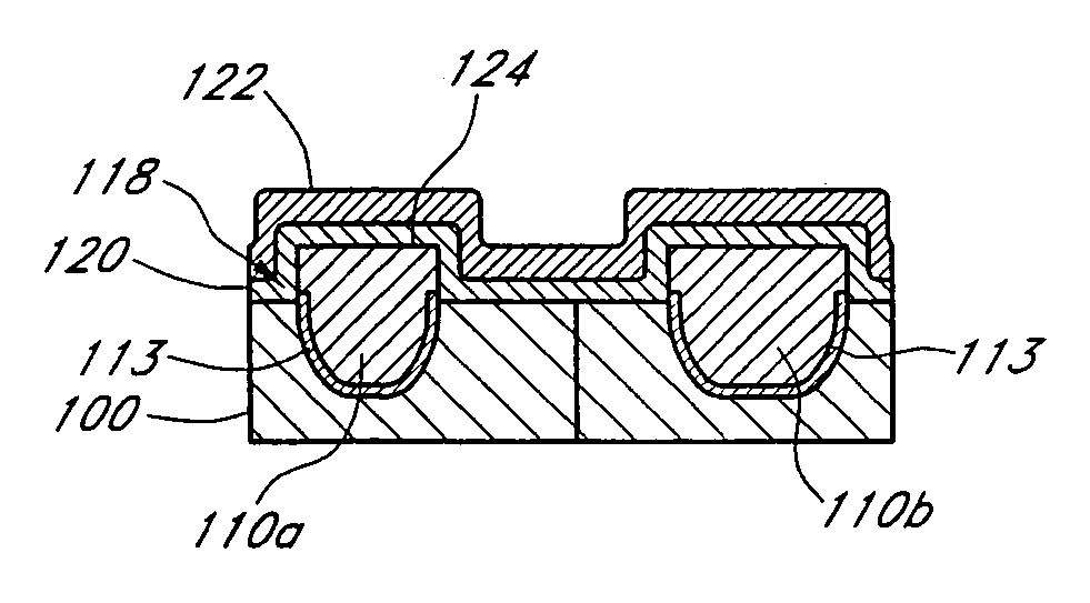
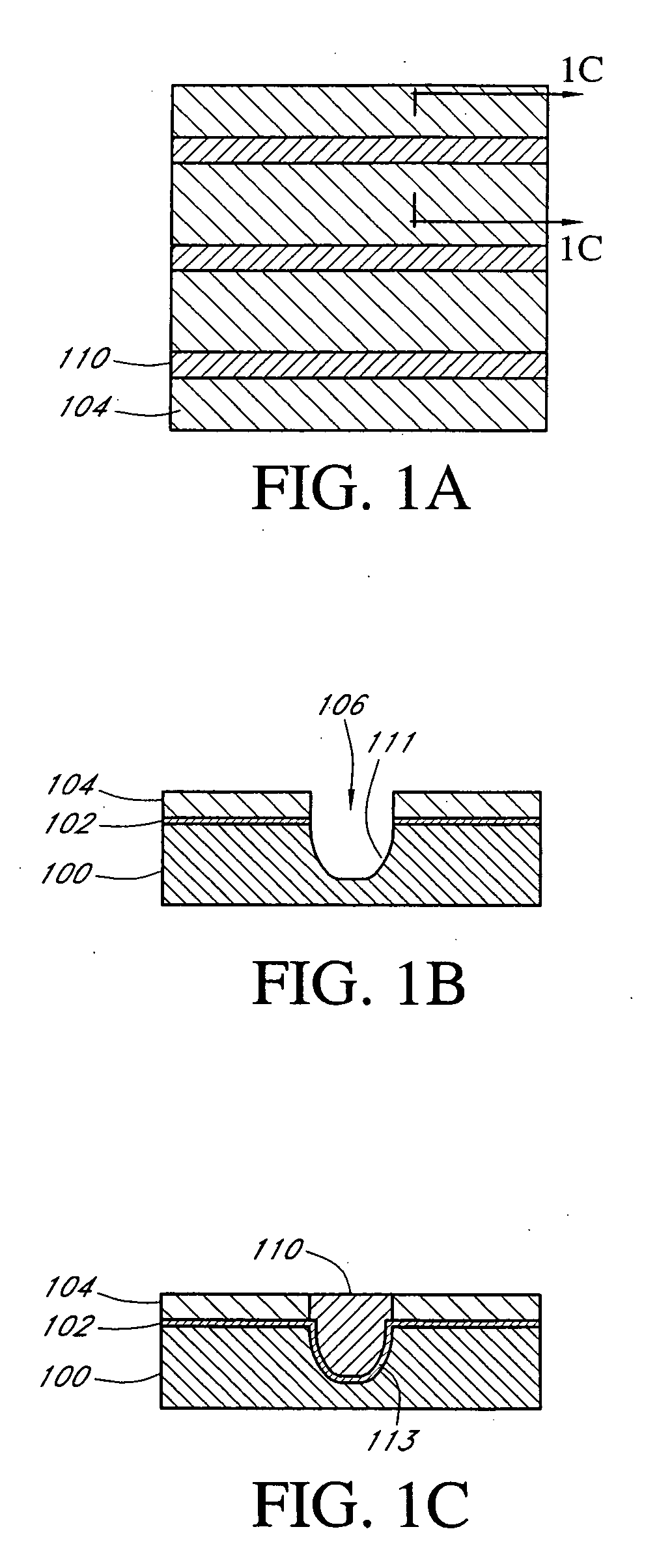
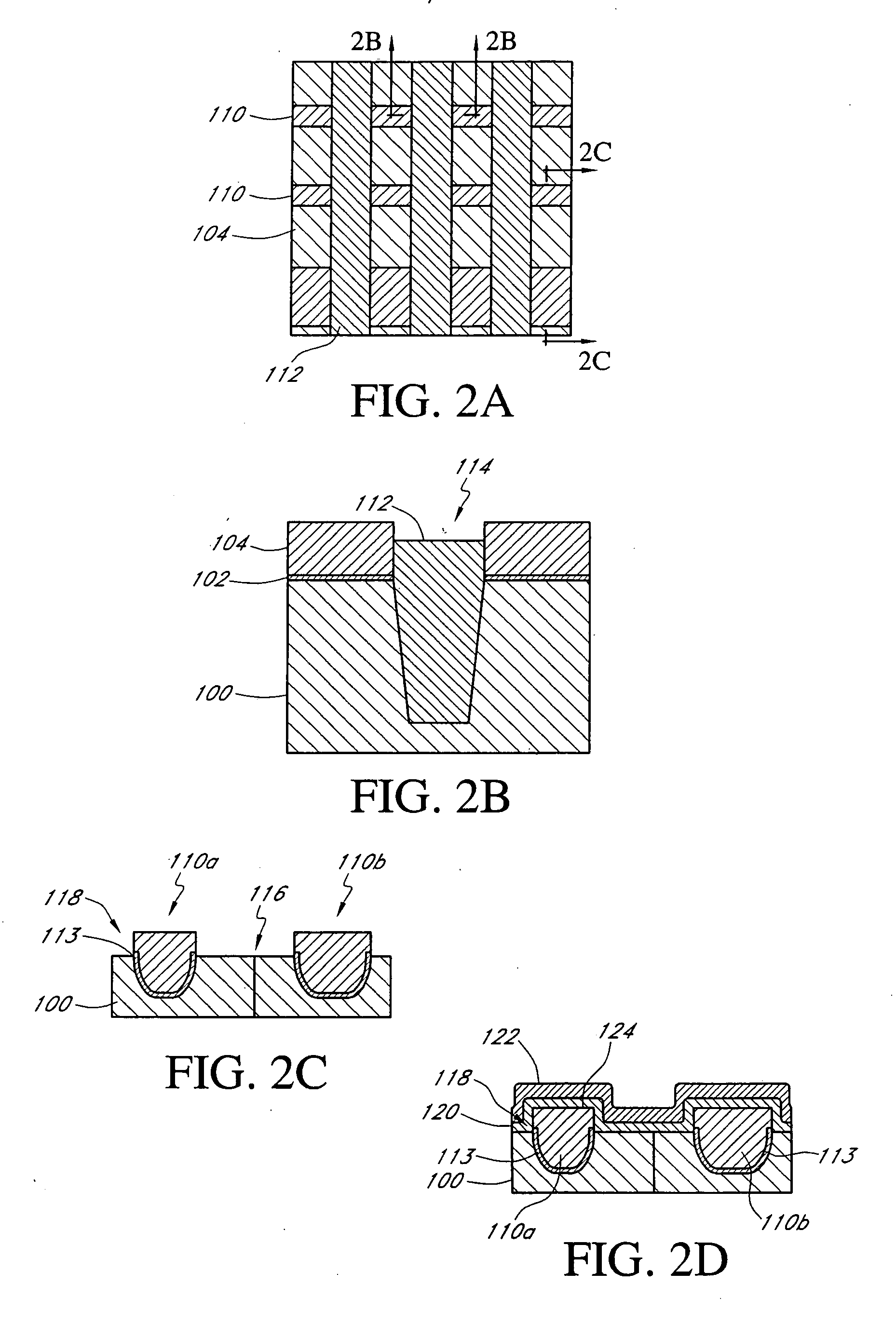
[0026] Referring initially to FIGS. 1A-1C, the initial process and steps to form a flash memory with recessed access device is illustrated. In this particular implementation, a pad oxide layer 102 is globally deposited over a semiconductor substrate 100 and then a masking layer, such as a nitride layer 104 is then deposited over the pad oxide 102. In one particular implementation, the pad oxide 102 is formed using a wet oxidation process such that the pad oxide has a thickness of approximately 100 Å and the nitride is deposited using a well-known process to have a thickness of approximately 700 Å.

[0027] As is illustrated in FIG. 1B, once the pad oxide 102 and the nitride layer 104 have been globally deposited on an upper surface of the semiconductor substrate 100, an opening or recess 106 is formed, using well known patterning and etching techniques, so as to define the recess 10...


PUM


Abstract

A flash memory device wherein the floating gate of the flash memory is defined by a recessed access device. The use of a recessed access device results in a longer channel length with less loss of device density. The floating gate can also be elevated above the substrate a selected amount so as to achieve a desirable coupling between the substrate, the floating gate and the control gate comprising the flash cell.

Description

BACKGROUND OF THE INVENTION [0001] 1. Field of the Invention [0002] The present invention relates to memory devices and, in particular, concerns a flash memory device formed with a recessed gate structure. [0003] 2. Description of the Related Art [0004] A wide variety of computer memory devices are now available for use in electrical circuits. A typical computer memory device is a DRAM circuit which offers a high density memory storage device. With all memory devices there is a desire for an increased density of memory devices per chip area. Unfortunately, with increased density of memory devices, the actual physical device dimensions become reduced which causes leakage problems and the like. [0005] One type of memory device which has become quite popular in the past few years is a flash memory device. A flash memory has the advantage of permitting global erasing of all of the cells and also has advantages in terms of processing in that the flash memory generally does not require a ...

Claims


Application Information

Patent Timeline
Patent Type & Authority Applications(United States)
IPC IPC(8): H01L21/336
CPCH01L21/28273H01L27/115H01L29/66825H01L27/11524H01L27/11521H01L29/40114H10B41/35H10B69/00H10B41/30H10B63/80
Inventor ABBOTT, TODD
Owner MICRON TECH INC
Why Eureka
Try Eureka