Protective coating for planarization

a protective coating and planarization technology, applied in the direction of basic electric elements, semiconductor/solid-state device manufacturing, electric devices, etc., can solve the problems of insufficient resolution and fidelity of existing techniques, large additional steps, and large expense, and achieve the effect of reducing the height of features and filler layers

Active Publication Date: 2007-03-01
MICRON TECH INC
View PDF80 Cites 235 Cited by
  • Summary
  • Abstract
  • Description
  • Claims
  • Application Information

AI Technical Summary

Benefits of technology

[0016] In some embodiments, a method of manufacturing computer memory is provided. The method can comprise: forming separated features in a memory array region; depositing a filler layer around and over the features in the memory array region and in a peripheral region such that the surface of the filler layer is less smooth than the surface of the peripheral region; forming a protective layer...

Problems solved by technology

Because many photoresist materials respond selectively to particular wavelengths, photolithography techniques each have a minimum pitch below which that particular photolithographic technique cannot reliably form features.
Due to factors such as geometric complexity and different requirements for critical dimensions in different parts of an integrated circuit, typically not all features of th...

Method used


Image

  • Protective coating for planarization
  • Protective coating for planarization
  • Protective coating for planarization

Examples


Embodiment Construction

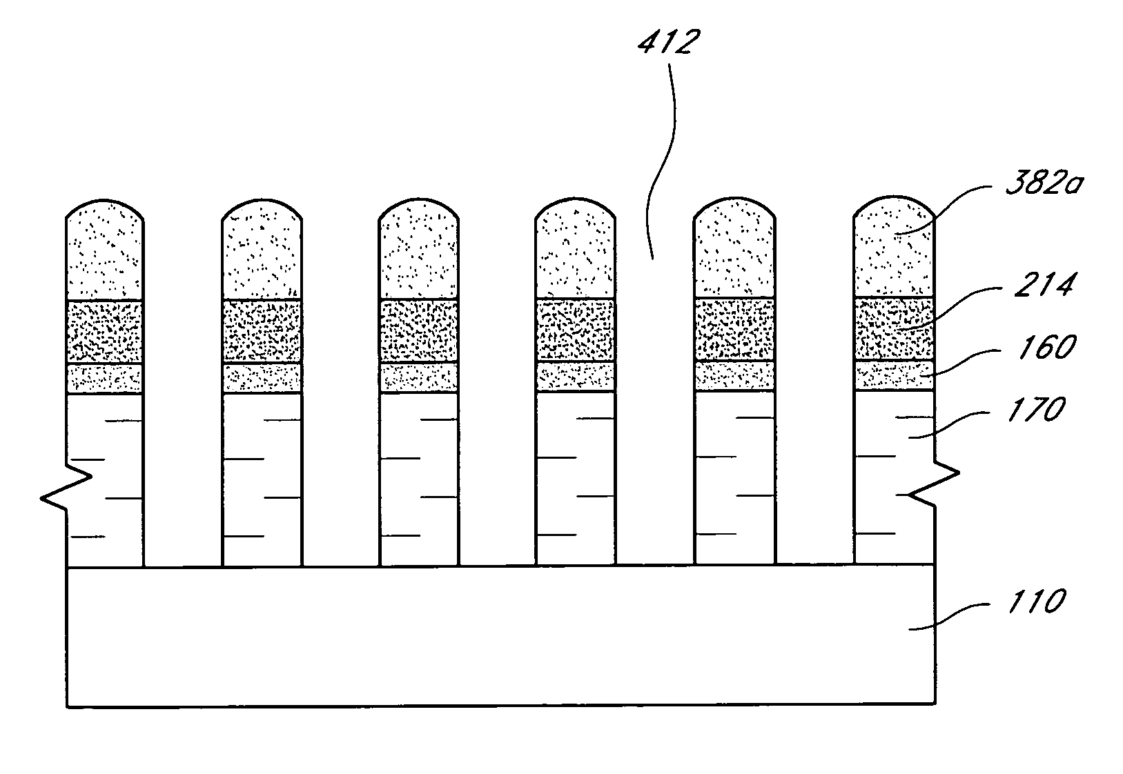
[0056] With reference to FIG. 2, a partially formed integrated circuit 100 is provided. A substrate 110 is provided below various masking layers 120-170. The layers 120-170 can be etched to form masks for patterning underlying layers or substrate 110. These masks can be used to form various features, as discussed below. The features can comprise portions of any of the following: one or multiple transistors, diodes, capacitors, conductive lines, gates, sources, drains, or contacts to any of the above. These components can comprise portions of DRAM or flash memory arrays, NOR logic arrays, NAND logic arrays, etc. In some embodiments, the features are formed from a substrate material that comprises a semi-conducting material. For example, the semi-conducting material can be silicon, silicon-germanium compounds, or III-V materials.

[0057] As used in this specification, the term “substrate” can refer not only to the substrate layer 110, but also to any layer that underlies another layer....


PUM

PropertyMeasurementUnit
Thicknessaaaaaaaaaa
Heightaaaaaaaaaa

Abstract

Various pattern transfer and etching steps can be used to create features. Conventional photolithography steps can be used in combination with pitch-reduction techniques to form superimposed, pitch-reduced patterns of crossing elongate features that can be consolidated into a single layer. Planarizing techniques using a filler layer and a protective layer are disclosed. Portions of an integrated circuit having different heights can be etched to a common plane.

Description

REFERENCE TO RELATED APPLICATIONS [0001] This application is related to the following: U.S. patent application Ser. No. 10 / 932,993 (MICRON.293A) filed Sep. 1, 2004; U.S. patent application Ser. No. 10 / 934,778 (MICRON.294A) filed Sep. 2, 2004; U.S. patent application Ser. No. 10 / 931,771 (MICRON.295A) filed Aug. 31, 2004; U.S. patent application Ser. No. 10 / 934,317 (MICRON.296A) filed Sep. 2, 2004; and U.S. patent application Ser. No. 11 / 134,982 (MICRON.317A) filed May 23, 2005. Each of the above-listed references is hereby incorporated by reference in its entirety and made part of this specification.BACKGROUND OF THE INVENTION [0002] 1. Field of the Invention [0003] The disclosed invention relates generally to integrated circuit fabrication, techniques for fabrication of computer memory, and masking techniques. [0004] 2. Description of the Related Art [0005] As a consequence of many factors, including demand for increased portability, computing power, memory capacity and energy effic...

Claims


Application Information

Patent Timeline
IPC IPC(8): H01L21/302
CPCH01L21/0337H01L21/31055H01L21/306H01L21/30625Y10T29/49146Y10T29/4922Y10T29/49155Y10T29/49176Y10T29/49128Y10T29/49224Y10T29/49172Y10T29/49151Y10T29/49171H01L21/31051H01L21/31111H01L21/31144
Inventor ABATCHEV, MIRZAFERWELLS, DAVIDZHOU, BAOSUOSUBRAMANIAN, KRUPAKAR M.
Owner MICRON TECH INC
Why Eureka
Try Eureka