Method of forming pitch multipled contacts

a technology of multiple contact and pitch, applied in the direction of basic electric elements, electrical equipment, semiconductor devices, etc., can solve the problems of not allowing the density of contact features to match, additional steps can involve considerable additional expense,

Active Publication Date: 2007-03-01
MICRON TECH INC
View PDF98 Cites 337 Cited by
  • Summary
  • Abstract
  • Description
  • Claims
  • Application Information

AI Technical Summary

Benefits of technology

[0016] In some embodiments, the invention comprises a method of forming elongate vias for an integrated circuit. The method can include depositing at least one layer of masking material over an underlying layer. The method can also include forming a first set of lines in a layer of masking material using conventional photolithography. Pitch-reduced spacer lines can be created that are elongate along an axis parallel to the first set of lines, and the spacer lines can give rise to a first pattern. A second pattern can also be formed using conventional lithography in a layer overlying the pitch-reduced lines. The second pattern can have an opening, and the opening can have a first width along an axis that is parallel to the elongate axis of the pitch-reduced lines. Furthermore, the first width can be definable without using pitch reduction techniques. Then, the insulating layer can be etched through a combined pattern defined by a superposition of the two patterns to create contact vias in the underlying layer.

Problems solved by technology

Because many photoresist materials respond selectively to particular wavelengths, photolithography techniques each have a minimum pitch below which that particular photolithographic technique cannot reliably form features.
Due to factors such as geometric complexity and different requirements for critical dimensions in different parts of an integrated circuit, typically not all features of the integrated circuit will be pitch multiplied.
Furthermore, pitch multiplication entails many additional steps relative to conventional lithography; the additional steps can involve considerable additional expense.
However, if some features of an integrated circuit are pitch multiplied, it is inconvenient if connecting features that interface with those features are not also pitch multiplied.
Conventional methods of forming contacts through insulating materials to create electrical connections between underlying and overlying circuit layers have not allowed the density of contact features to match the density of the features intended to be connected by those contact features.

Method used


Image

  • Method of forming pitch multipled contacts
  • Method of forming pitch multipled contacts
  • Method of forming pitch multipled contacts

Examples


Embodiment Construction

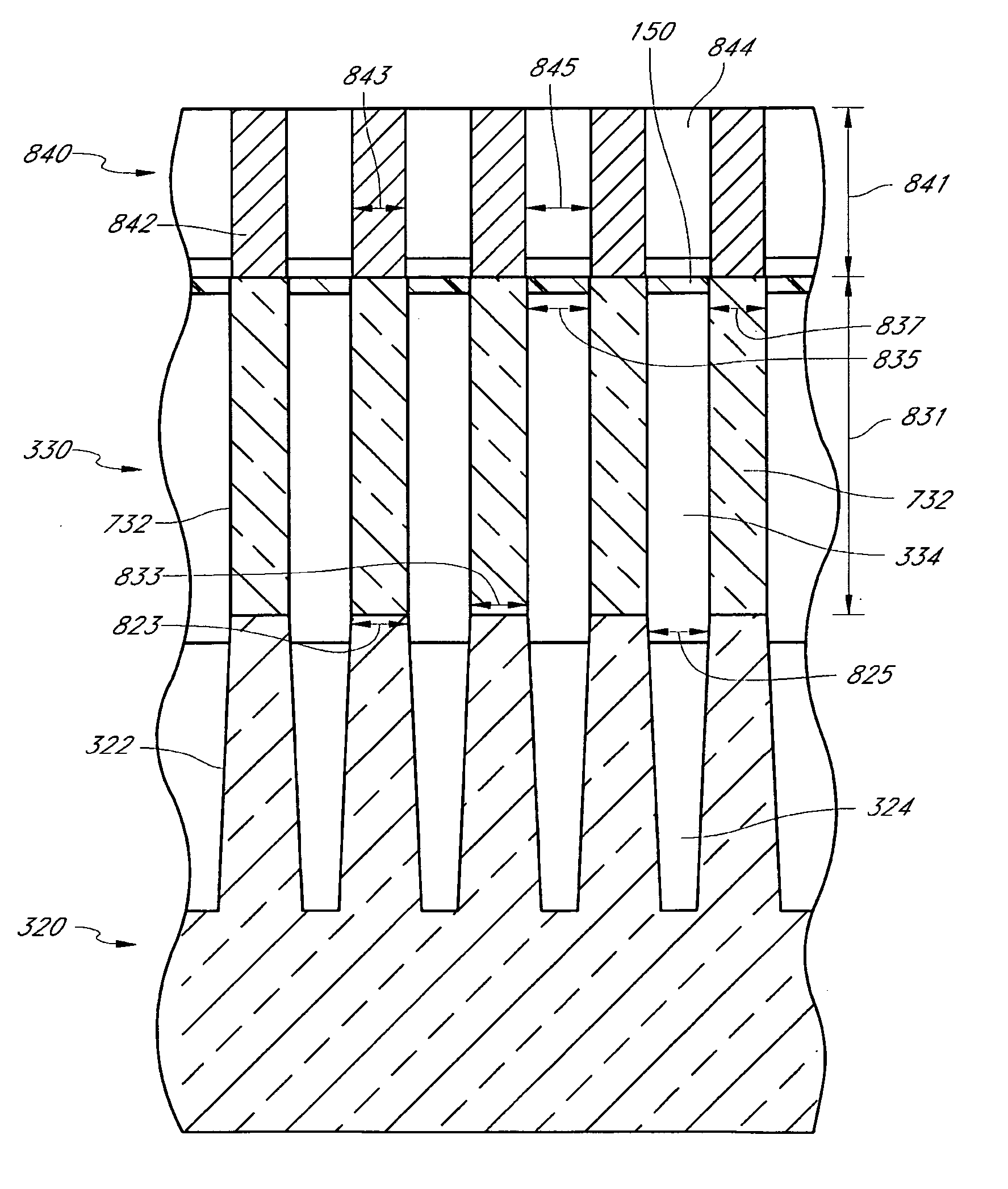
[0042] With reference to FIG. 2, a portion of an integrated circuit is shown in cross-section. In an underlying substrate level 220, the features 222 are formed to extend upwardly. In some embodiments, the features 222 taper so that the features 222 have a thinner cross section at their upper extremity than they do at their bottom extremity. This tapered shape can be a result of an etching step with a lateral etch component due to the upper portions of the features being exposed to an etching chemistry for a longer period of time than the lower portions. The features 222 are advantageously longer in a dimension into and out of the plane of the paper, so that the critical dimension of the features 222 is different in the X and Y dimensions. Transistor pillars (not shown) preferably protrude above the ridges defined by the features at other locations. U.S. patent application Ser. No. 11 / 010,752, to Haller, filed Dec. 13, 2004, and assigned to Micron, Inc. (Atty. docket No. MICRON.288A...


PUM


Abstract

Methods of forming electrically conductive and/or semiconductive features for use in integrated circuits are disclosed. Various pattern transfer and etching steps can be used, in combination with pitch-reduction techniques, to create densely-packed features. The features can have a reduced pitch in one direction and a wider pitch in another direction. Conventional photo-lithography steps can be used in combination with pitch-reduction techniques to form elongate, pitch-reduced features such as bit-line contacts, for example.

Description

REFERENCE TO RELATED APPLICATIONS [0001] This application is related to the following: U.S. patent application Ser. No. 10 / 931,772 to Abatchev et al., filed Aug. 31, 2004, entitled Critical Dimension Control, (Atty. docket No. MICRON.286A; Micron Ref. No. 2003-1348); U.S. patent application Ser. No. 11 / 010,752, to Haller, filed Dec. 13, 2004, and assigned to Micron, Inc. (Atty. docket No. MICRON.288A; Micron Ref. No. 2003-1333); U.S. patent application Ser. No. 10 / 922,583, filed Aug. 19, 2004, and assigned to Micron, Inc. (Atty. Docket No. MICRON.290A; Micron Ref. No. 2003-1476); U.S. patent application Ser. No. 10 / 932,993 to Abatchev et al., filed Sep. 1, 2004, entitled Mask Material Conversion, (Atty. docket No. MICRON.293A; Micron Ref. No. 2003-1435); U.S. patent application Ser. No. 10 / 934,778 to Abatchev et al., filed Sep. 2, 2004, entitled Method for Integrated Circuit Fabrication Using Pitch Multiplication, (Atty. docket No. MICRON.294A; Micron Ref. No. 2003-1446); U.S. paten...

Claims


Application Information

Patent Timeline
Patent Type & Authority Applications(United States)
IPC IPC(8): H01L21/311
CPCH01L21/0337H01L21/0338H01L21/31144H01L21/76816H01L27/1052H01L27/10888H01L27/11521H01L21/3088H01L21/76805H01L21/76838H10B99/00H10B12/485H10B41/30H01L21/768H01L21/033
Inventor TRAN, LUAN C.
Owner MICRON TECH INC
Why Eureka
Try Eureka