
Test mode to force generation of all possible correction codes in an ECC memory

a technology of error correction and test mode, applied in the field of test mode, can solve the problem that all errors capable of being corrected by error correction data may be forced

Inactive Publication Date: 2007-03-01
MICRON TECH INC
View PDF36 Cites 16 Cited by
  • Summary
  • Abstract
  • Description
  • Claims
  • Application Information

AI Technical Summary

Benefits of technology

[0004] The present disclosure provides a method and apparatus for quickly characterizing an aspect of a memory device, i.e., to characterize the time needed to correct a worst case data error with onboard error correcting circuitry. Individual bits can be flipped (their state changed from logic 1 to logic zero or vice versa) to mimic an error by forcing the test data to the state corresponding to the bit desired to be flipped. By flipping various bits or combinations of bits, various predetermined errors can be forced. By measuring the time delay between when uncorrected data is output from the memory device and when corrected data is output, the time the error correction circuitry takes to correct each of the forced errors can be measured and the part characterized according to the various measurements.

Problems solved by technology

The errors are forced by manipulating at least one bit of the test data or error correction data to produce a predetermined error.
All of the errors capable of being corrected by the error correction data may be forced.

Method used


Image

  • Test mode to force generation of all possible correction codes in an ECC memory
  • Test mode to force generation of all possible correction codes in an ECC memory
  • Test mode to force generation of all possible correction codes in an ECC memory

Examples


Embodiment Construction

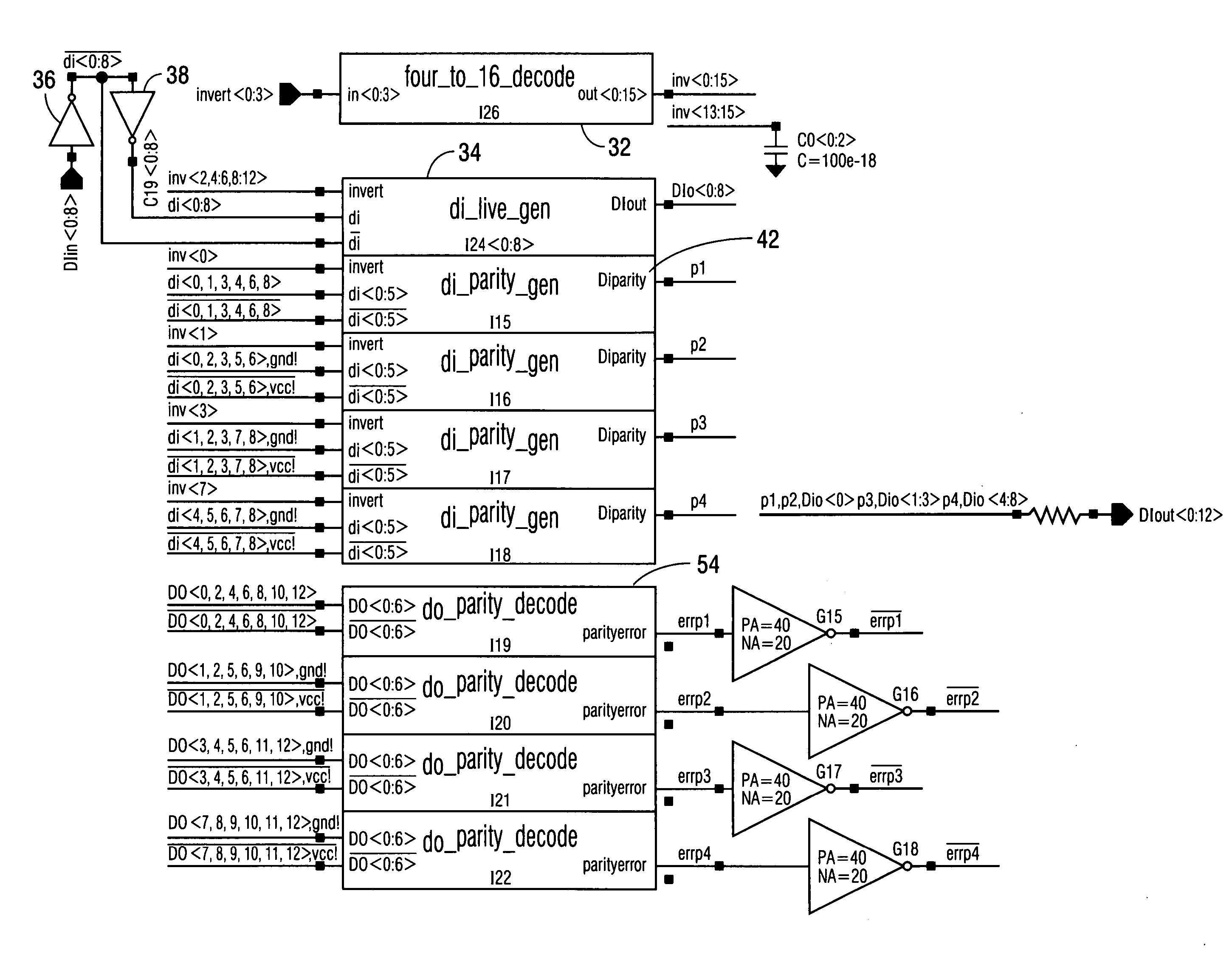
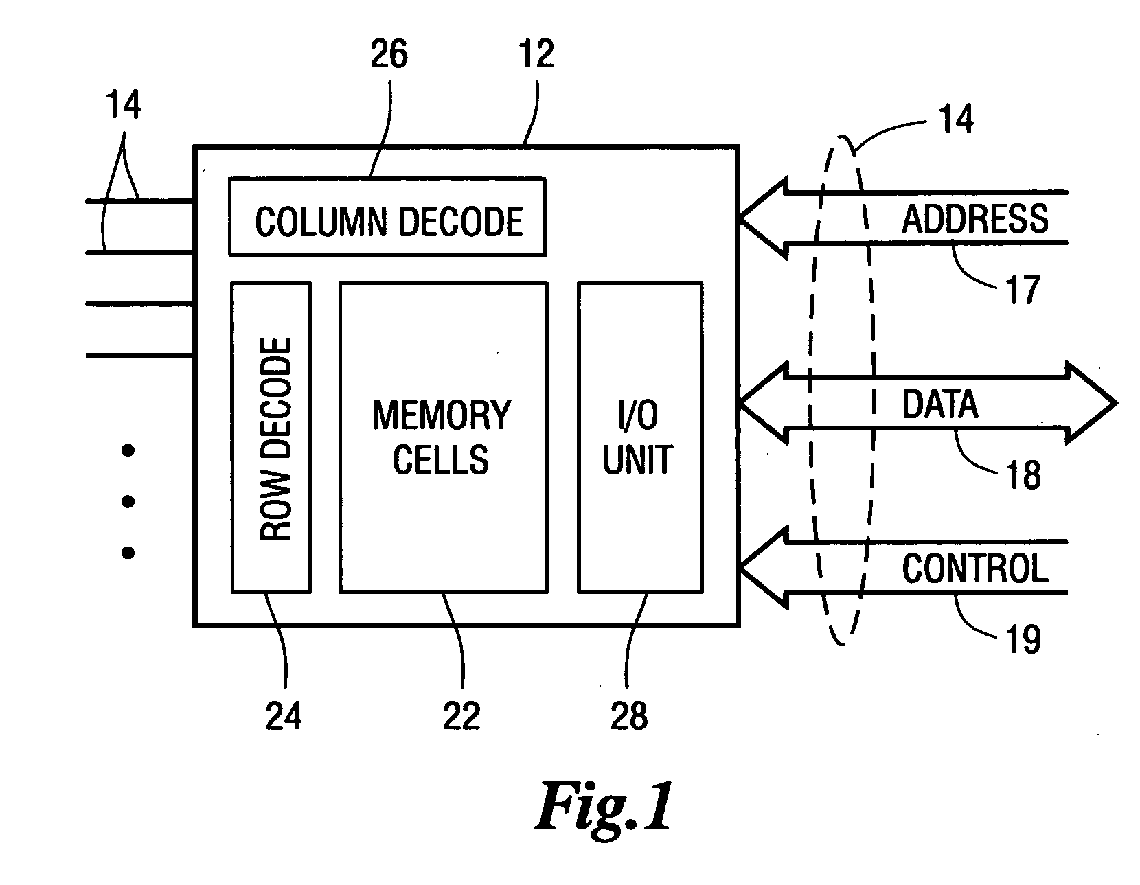
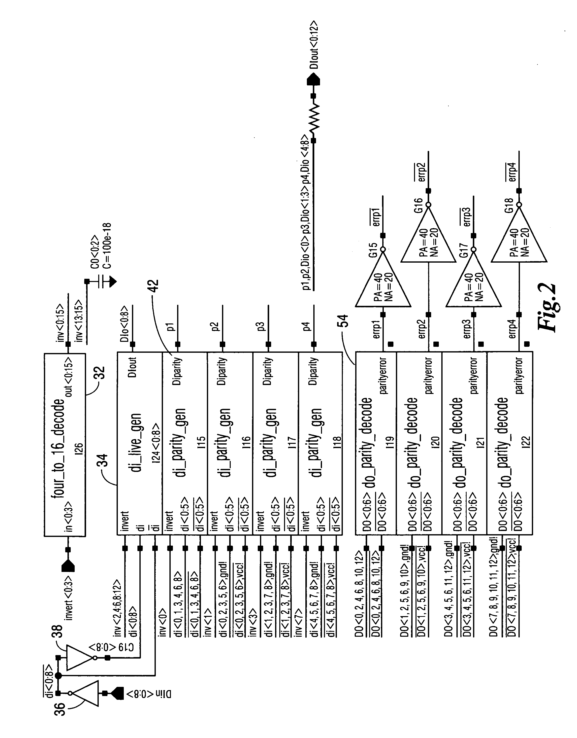
[0017] Memory devices are electronic devices that are widely used in many electronic products and computers to store data. A memory device is a semiconductor electronic device that includes a number of memory cells, each cell storing one bit of data. The data stored in the memory cells can be read during a read operation. FIG. 1 is a simplified block diagram showing a memory chip or memory device 12. The memory chip 12 may be part of a DIMM (dual in-line memory module) or a PCB (printed circuit board) containing many such memory chips (not shown in FIG. 1). The memory chip 12 may include a plurality of pins or ball contacts 14 located outside of chip 12 for electrically connecting the chip 12 to other system devices. Some of those pins 14 may constitute memory address pins or address bus 17, data (DQ) pins or data bus 18, and control pins or control bus 19. It is evident that each of the reference numerals 17-19 designates more than one pin in the corresponding bus. Further, it is u...


PUM


Abstract

The present disclosure enables individual bits of a data signal to be flipped (their state changed from logic one to logic zero or vice versa) to mimic an error. By flipping various bits or combinations of bits, various predetermined errors can be forced. By measuring the time delay between when uncorrected data is output from the memory device and when corrected data is output, the time the error correction circuitry takes to correct each of the forced errors can be measured and the part characterized according to the various measurements. Because of the rules governing abstracts, this abstract should not be used to construe the claims.

Description

BACKGROUND OF THE INVENTION [0001] The present disclosure is directed generally to test modes and, more particularly, to test modes used in connection with error correction codes. [0002] It is known in the prior art to conduct tests of memory devices to insure that the part is good. Such tests typically comprise generating a test pattern, writing the test pattern to the memory array, reading the written test pattern, and comparing the written test pattern with the read test pattern. Comparison of the aforementioned two test patterns will identify any memory locations in the array which are malfunctioning. [0003] In addition to the kind of test previously described, other types of tests are performed on parts, particularly new parts, for the purpose of characterizing the part. After the part has been characterized, the test may be performed randomly on various numbers of parts to insure that each batch or lot of parts continues to meet the established parameters for the part. BRIEF S...

Claims


Application Information

Patent Timeline
Patent Type & Authority Applications(United States)
IPC IPC(8): G06F11/00
CPCG06F11/1048G11C2029/0411G11C29/42G06F11/2215
Inventor GANS, DEAN
Owner MICRON TECH INC
Learn More