Optical coupling device and electronic apparatus using same
- Summary
- Abstract
- Description
- Claims
- Application Information
AI Technical Summary
Benefits of technology
Problems solved by technology
Method used
Image

Examples
embodiment 1
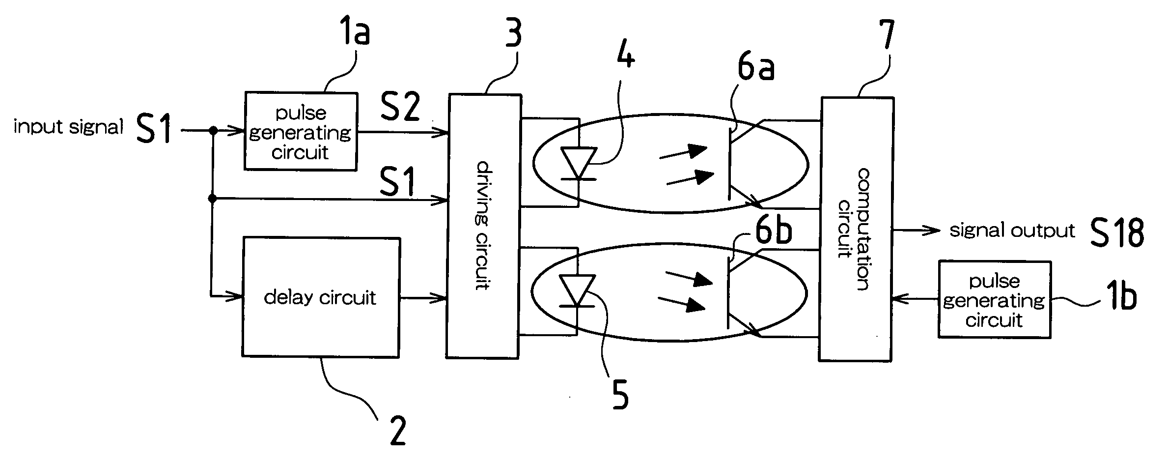
[0025]FIG. 1 is a functional block diagram of an optical coupling device according to Embodiment 1.
[0026] In the optical coupling device of Embodiment 1, an input side is configured with a pulse generating circuit 1a, a delay circuit 2, a driving circuit 3, and two light emitting elements 4 and 5 connected to the driving circuit 3, and an output side is configured with two light receiving elements 6a and 6b connected to a computation circuit 7, and a pulse generating circuit 1b.
[0027] An input signal S1 is input to the driving circuit 3 and to the delay circuit 2, and is further input to the pulse generating circuit 1a, which generates a clock pulse signal. The pulse generating circuit 1a generates a clock pulse signal S2 with a high speed synchronized with the input signal S1, and this is input to the driving circuit 3. The delay circuit 2, after delaying the input signal S1 for ½ the pulse of the clock pulse signal S2, inputs the input signal S1 to the driving circuit 3. The dri...
embodiment 2
[0043] Next is a description of an optical coupling device according to Embodiment 2 of the present invention.
[0044]FIG. 4 is a functional block diagram of the optical coupling device according to Embodiment 2 of the present invention.
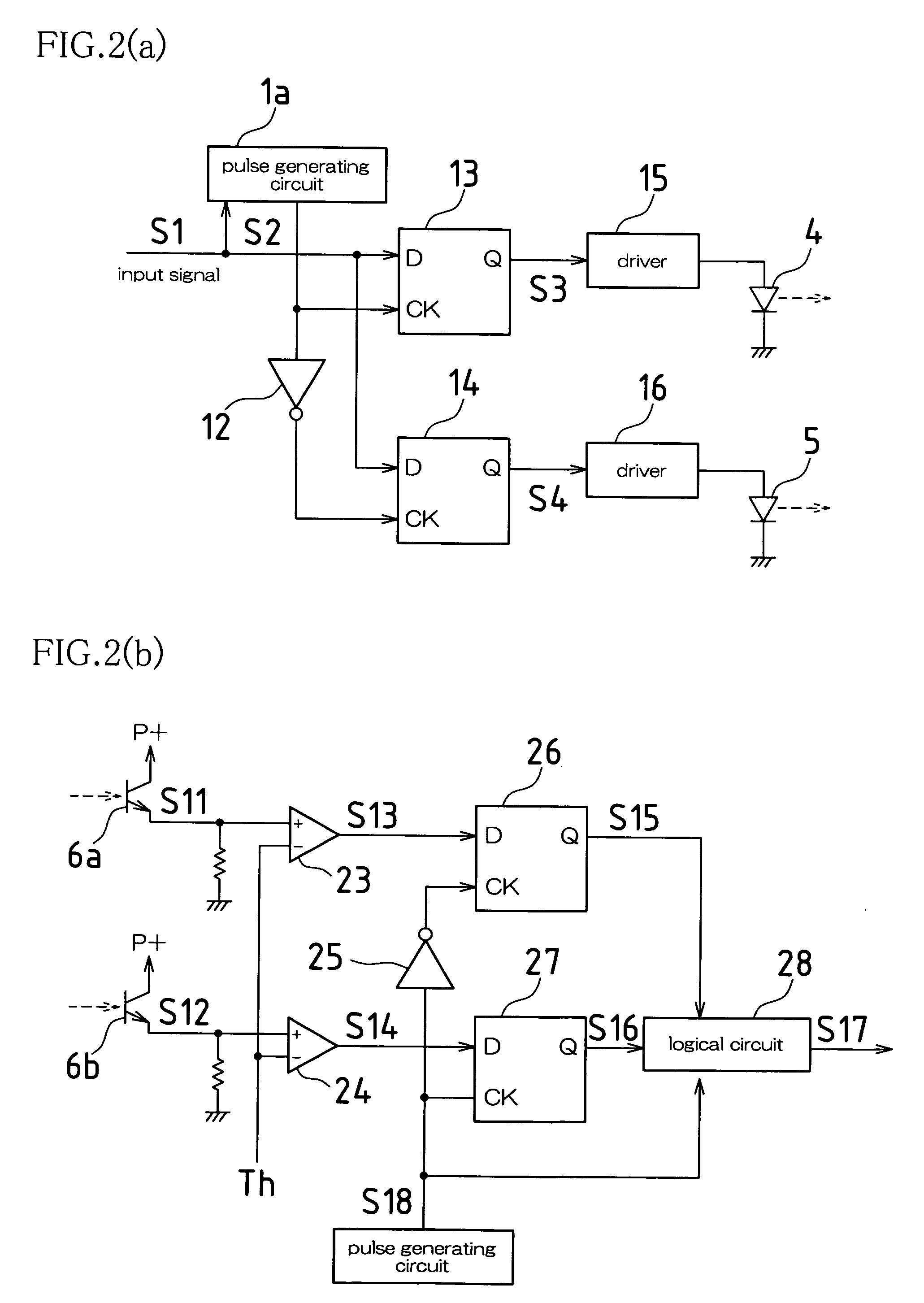
[0045] In Embodiment 2, the two LEDs 4 and 5 have different wavelengths, and with respect to the output side (the light receiving side), light receiving faces are manufactured at two locations on a single chip, and by providing sensitivity to the wavelengths of LEDs 4 and 5 in the each respective light receiving face, the light receiving element 6 can be formed with a single chip. The driving method in Embodiment 2 is the driving method according to the timing chart shown in FIG. 3, and so a description thereof is omitted here.
[0046] In above Embodiment 1, because two pairs of a light emitting element and a light receiving element need to be manufactured in a single package, and in order to prevent erroneous operation it is necessary to design such ...
PUM
 Abstract
Description
Claims
Application Information
 - R&D Engineer
- R&D Manager
- IP Professional
- Industry Leading Data Capabilities
- Powerful AI technology
- Patent DNA Extraction
Browse by: Latest US Patents, China's latest patents, Technical Efficacy Thesaurus, Application Domain, Technology Topic.
© 2024 PatSnap. All rights reserved.Legal|Privacy policy|Modern Slavery Act Transparency Statement|Sitemap