

Scan driving circuit and organic light emitting display device using the same
a driving circuit and display device technology, applied in the direction of instruments, computing, electric digital data processing, etc., can solve the problems of increasing power consumption, static current flow, and circuit may be erroneously operated, and achieve the effect of reducing power consumption
- Summary
- Abstract
- Description
- Claims
- Application Information
AI Technical Summary
Benefits of technology
Problems solved by technology
Method used
Image

Examples
first embodiment
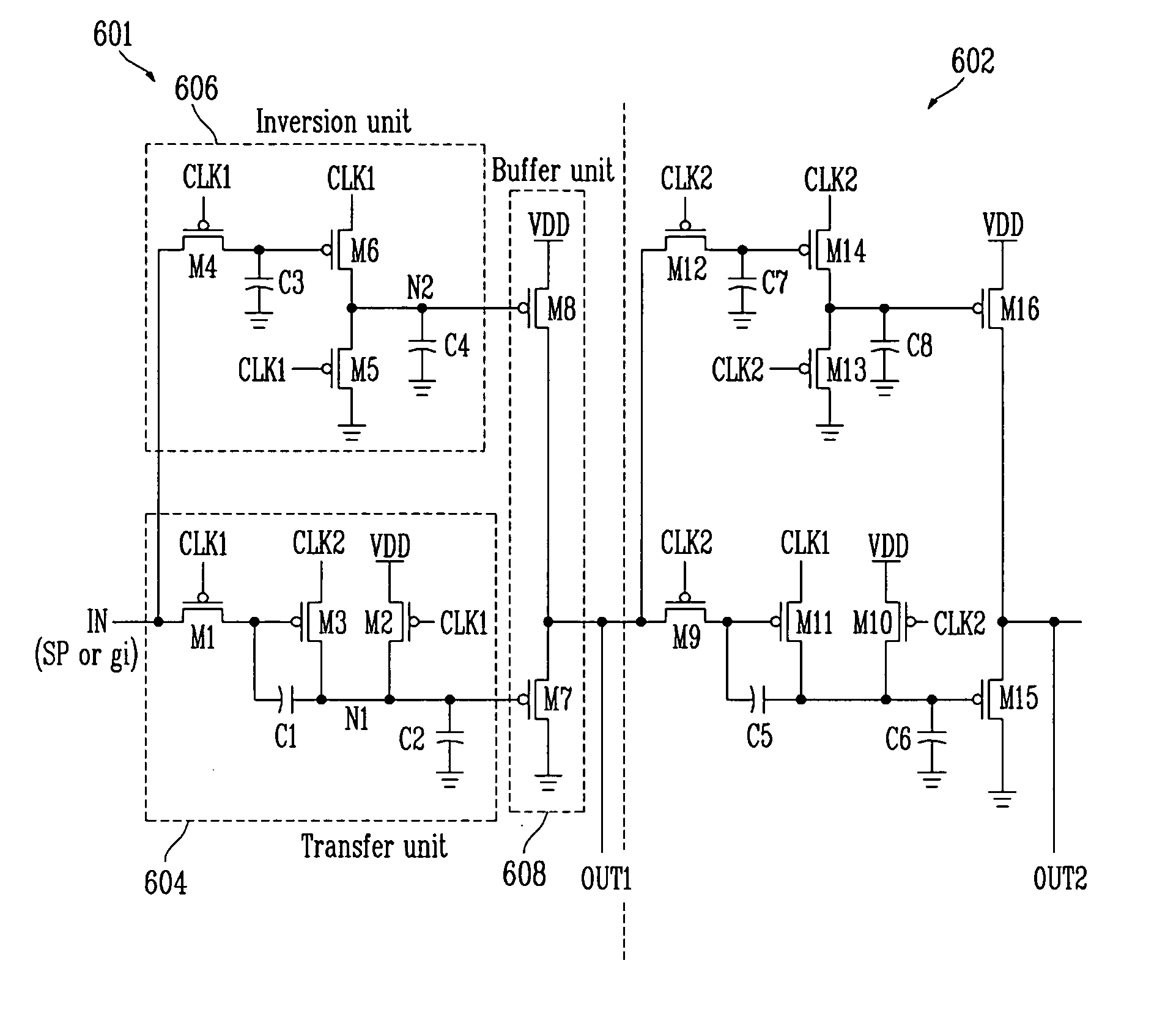
[0053]FIG. 6 is a circuit diagram of a scan driving circuit according to the present invention, which shows a detailed circuit arrangement of adjacent odd-numbered and even-numbered stages 601 and 602 in the scan driving circuit 10 of FIG. 5. FIG. 7 is an input / output waveform diagram of the stages shown in FIG. 6.
[0054] As shown in FIG. 6, the first embodiment of the present invention is realized with PMOS transistors. The PMOS transistors of each stage sequentially transfer a low-level output signal gi of a previous stage through a scan driving circuit, for example the scan driving circuit 10. That is, as shown FIG. 7, the scan driving circuit as described in the embodiments of the present invention outputs a high-level signal OUT1, OUT2 to the display region of an active matrix display device for most of the time, and sequentially outputs a low-level pulse or output signal gi through a plurality of stages. The notations OUT1 and OUT2 are used in this application to refer to both ...
second embodiment
[0082]FIG. 8 is a circuit diagram of the scan driving circuit according to the present invention, which shows a detailed circuit arrangement of adjacent odd-numbered and even-numbered stages in the scan driving circuit 10 of FIG. 5.
[0083] Like or same elements to the elements used in the first embodiment of FIG. 6 are designated by the same reference numerals and labels, and a detailed description of these elements is omitted.
[0084] As shown in FIG. 8, the seventh PMOS transistor M7 is removed from the buffer unit of the odd-numbered stage 601 of the first embodiment to arrive at an odd-numbered stage 801 of the second embodiment.
[0085] The removal of the seventh PMOS transistor M7 is performed for switching an output voltage of each state to the range of voltage of the first voltage source VDD. In the circuit 601 of the first embodiment, a high level of the output voltage OUT1 is nearly identical with the voltage level of the first voltage source VDD but a low level of the output...
third embodiment
[0088]FIG. 9 is a circuit diagram of odd and even stages of the scan driving circuit according to the present invention, which shows a detailed circuit arrangement of adjacent odd-numbered and even-numbered stages in the scan driving circuit 10 of FIG. 5.
[0089] Like or same elements to the elements used in the first and second embodiments of FIG. 6 and FIG. 8 are designated by the same reference numerals and labels, and a detailed description of these elements is omitted.
[0090] As shown in FIG. 9, the third embodiment, like the second embodiment, removes the seventh PMOS transistor M7 of the odd-numbered stage 601 and the fifteenth PMOS transistor M15 of the even-numbered stage 602 of the first embodiment. Further, first and fourth transistors M1 and M4 and ninth and twelfth transistors M9 and M12 that are controlled by the same signal in the first and second embodiments, are integrated into one transistor in respectively an odd-numbered stage 901 and an even-numbered stage 902 of ...
PUM
 Abstract
Description
Claims
Application Information