Electrode structure and method of manufacturing the same, phase-change memory device having the electrode structure and method of manufacturing the same

a technology of phase-change memory and electrode structure, which is applied in the direction of basic electric elements, semiconductor devices, electrical equipment, etc., can solve the problems that flash memory devices may require a longer amount of time for reading, and achieve the effects of increasing the structural stability of the electrode structure, reducing the risk of etching, and improving the etching selectivity

Inactive Publication Date: 2007-03-15
SAMSUNG ELECTRONICS CO LTD
View PDF2 Cites 19 Cited by
  • Summary
  • Abstract
  • Description
  • Claims
  • Application Information

AI Technical Summary

Benefits of technology

[0037] According example embodiments of the present invention, first and second insulation layer patterns surround and support an electrode such that structural stability of an electrode structure may increase. In a chemical mechanical polishing process for forming the electrode, the second insulation layer pattern has a relatively higher etching selectivity relative to that of the electrode. As such, the second insulation layer may have a more uniform thickness and roughness of the electrode also may decrease. When the electrode structure is applied to a phase-change memory device, the phase-change memory device may have a more consistent resistance and increased characteristics.

Problems solved by technology

Flash memory devices may require a longer amount of time for reading or writing data such that alternative memory devices may be necessary.

Method used


Image

  • Electrode structure and method of manufacturing the same, phase-change memory device having the electrode structure and method of manufacturing the same
  • Electrode structure and method of manufacturing the same, phase-change memory device having the electrode structure and method of manufacturing the same
  • Electrode structure and method of manufacturing the same, phase-change memory device having the electrode structure and method of manufacturing the same

Examples


Embodiment Construction

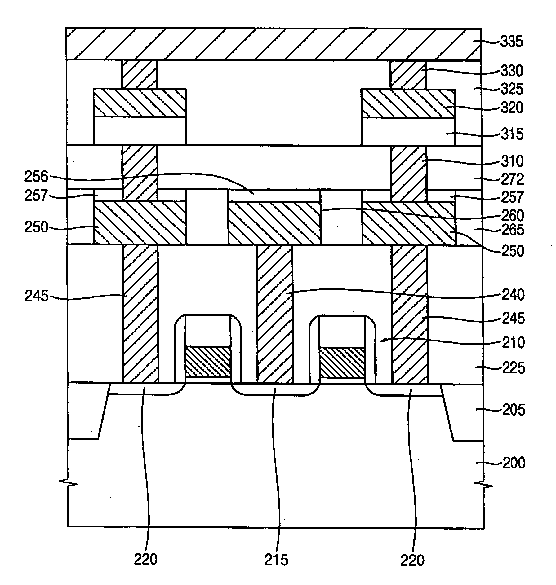
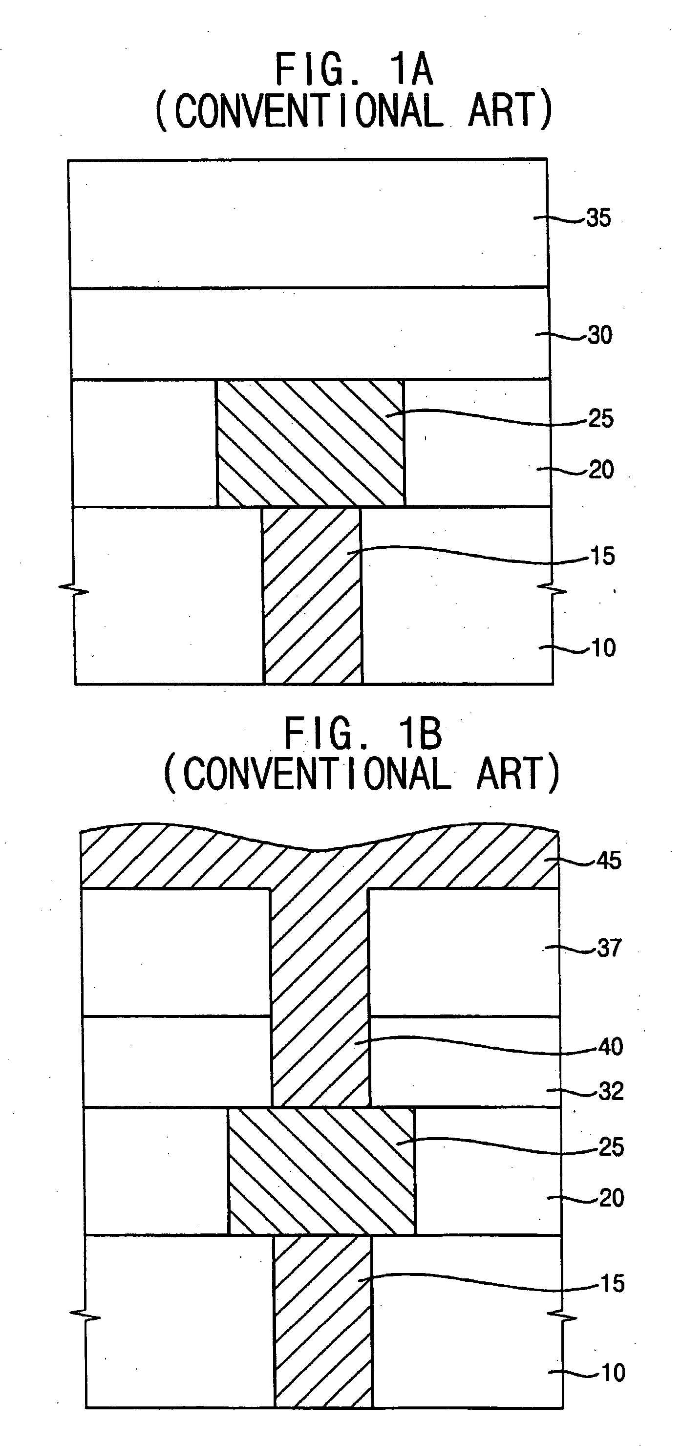
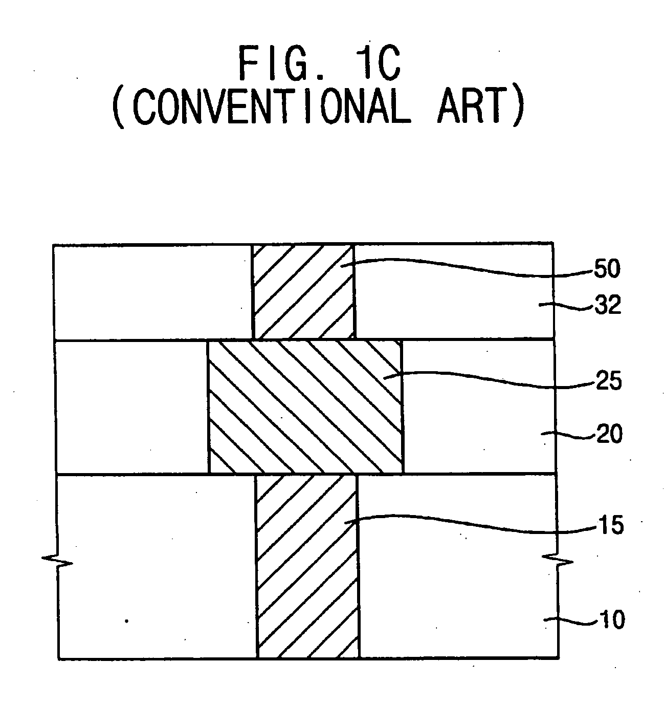
[0045] Various example embodiments of the present invention will now be described more fully with reference to the accompanying drawings in which some example embodiments of the invention are shown. In the drawings, the thicknesses of layers and regions may be exaggerated for clarity.

[0046] Detailed illustrative embodiments of the present invention are disclosed herein. However, specific structural and functional details disclosed herein are merely representative for purposes of describing example embodiments of the present invention. This invention may, however, may be embodied in many alternate forms and should not be construed as limited to only the embodiments set forth herein.

[0047] Accordingly, while example embodiments of the invention are capable of various modifications and alternative forms, embodiments thereof are shown by way of example in the drawings and will herein be described in detail. It should be understood, however, that there is no intent to limit example emb...


PUM


Abstract

Example embodiments of the present invention relate to an electrode structure, a method of manufacturing the electrode structure, a phase-change memory device having the electrode structure and a method of manufacturing the phase-change memory device. The electrode structure may include a pad, a first insulation layer pattern, a second insulation layer pattern and/or an electrode. The first insulation layer pattern may be formed on the pad. The first insulation layer pattern may have a first opening that partially exposes the pad. The second insulation layer pattern may be formed on the first insulation layer pattern. The second insulation layer pattern may have a second opening connected to the first opening. The electrode may be formed on the pad and filling the first and the second openings.

Description

PRIORITY STATEMENT [0001] This application claims the benefit of priority under 35 U.S.C. § 119 to Korean Patent Application No. 2005-63326, filed on Jul. 13, 2005, the contents of which are herein incorporated by references in their entirety. BACKGROUND OF THE INVENTION [0002] 1. Field of the Invention [0003] Example embodiments of the present invention relate to an electrode structure, a method of manufacturing the electrode structure, a phase-change memory device having the electrode structure and a method of manufacturing the phase-change memory device. Other example embodiments of the present invention relate to an electrode structure having increased characteristics, a method of manufacturing the electrode structure, a phase-change memory device having the electrode structure and a method of manufacturing the phase-change memory device. [0004] 2. Description of the Related Art [0005] There are several types of semiconductor memory devices (e.g., static random access memory (SR...

Claims


Application Information

Patent Timeline
Patent Type & Authority Applications(United States)
IPC IPC(8): H01L29/76
CPCH01L21/76834H01L27/2436H01L45/06H01L45/1233H01L45/1675H01L45/143H01L45/144H01L45/148H01L45/16H01L45/1253H10B63/30H10N70/231H10N70/826H10N70/841H10N70/8825H10N70/8828H10N70/884H10N70/011H10N70/063H01L29/40114
Inventor MIN, CHUNG-KIKO, YONG-SUNKIM, KYUNG-HYUN
Owner SAMSUNG ELECTRONICS CO LTD
Why Eureka
Try Eureka