Semiconductor FinFET structures with encapsulated gate electrodes and methods for forming such semiconductor FinFET structures
- Summary
- Abstract
- Description
- Claims
- Application Information
AI Technical Summary
Benefits of technology
Problems solved by technology
Method used
Image

Examples
Embodiment Construction
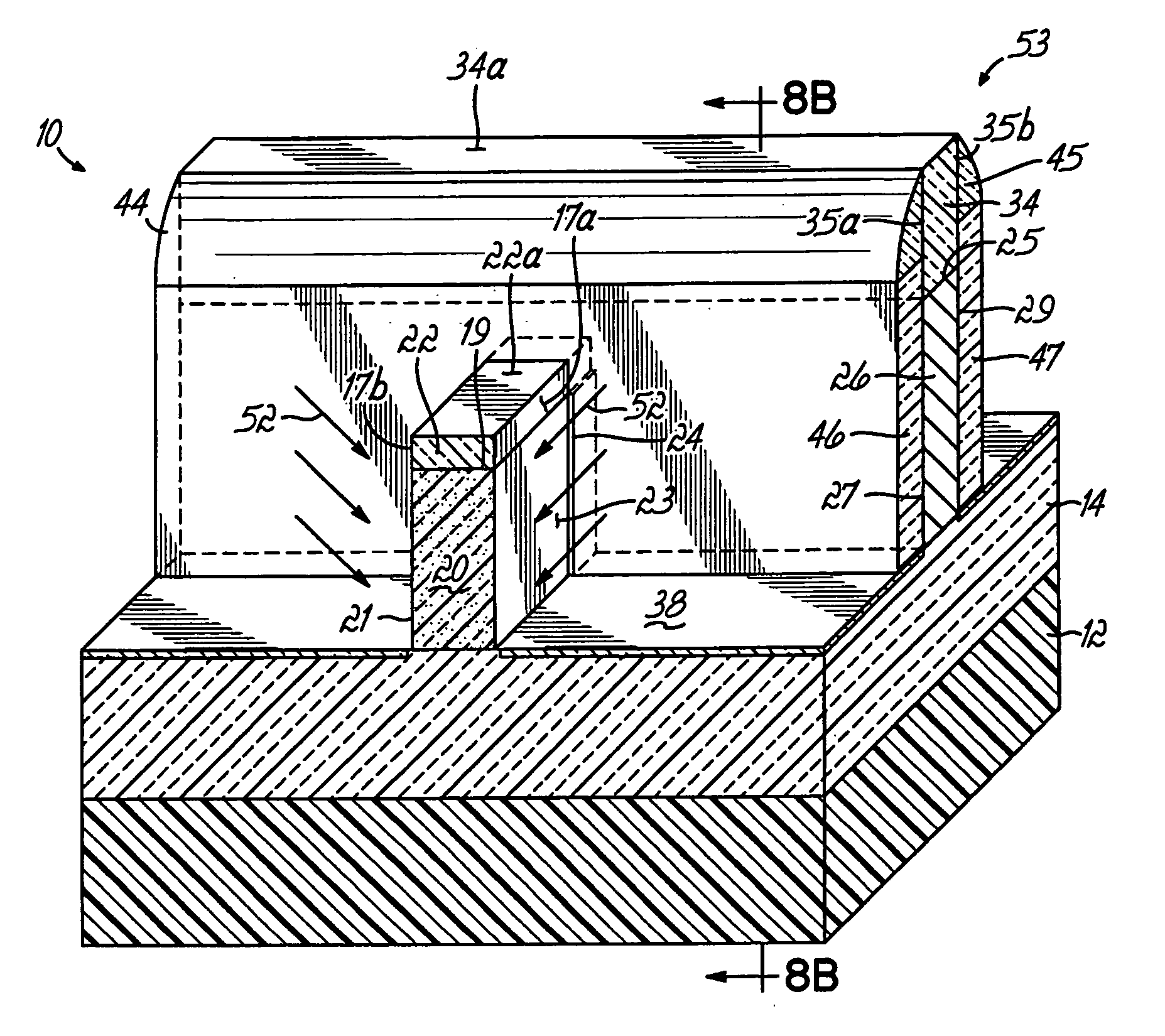
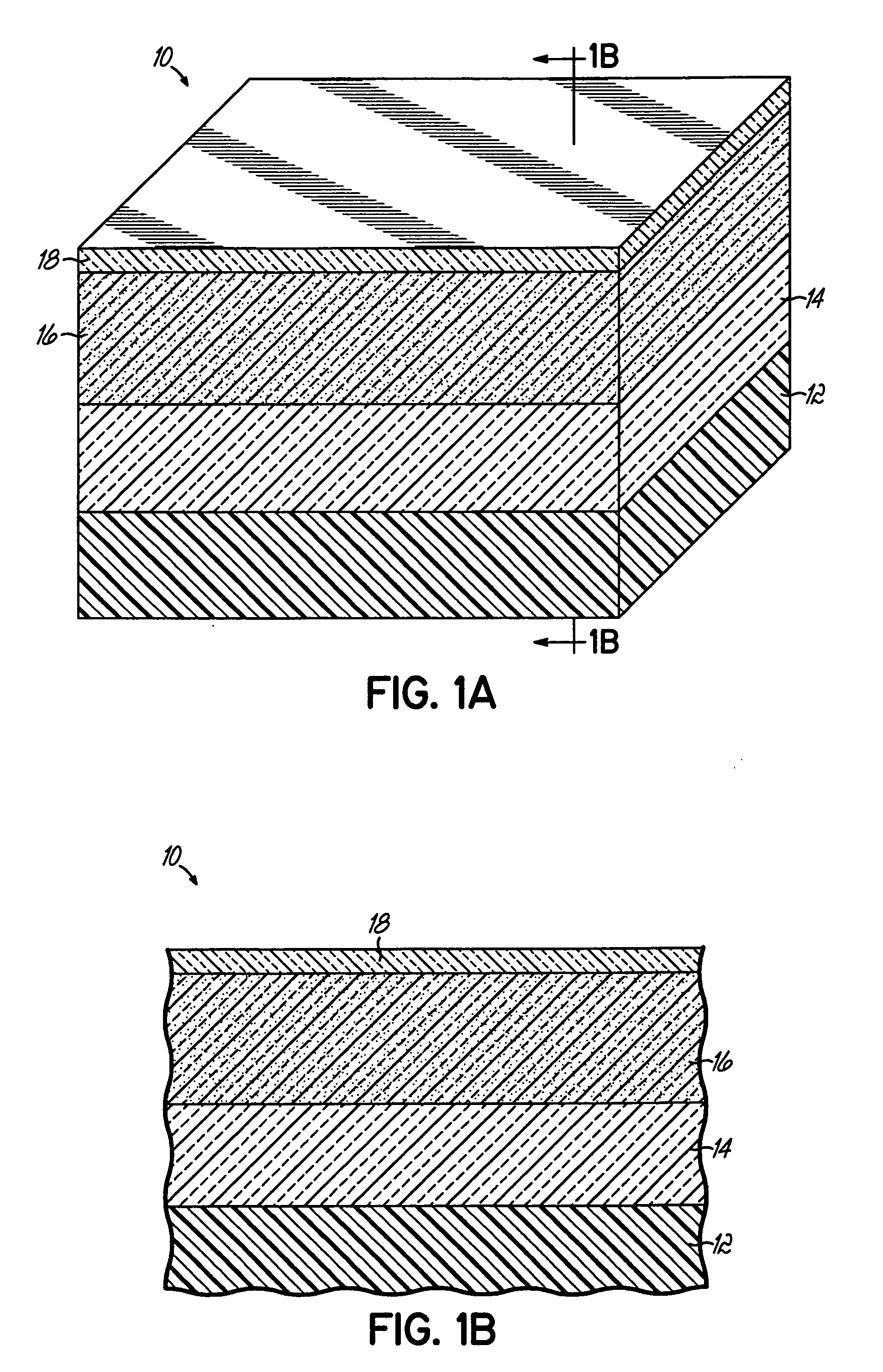
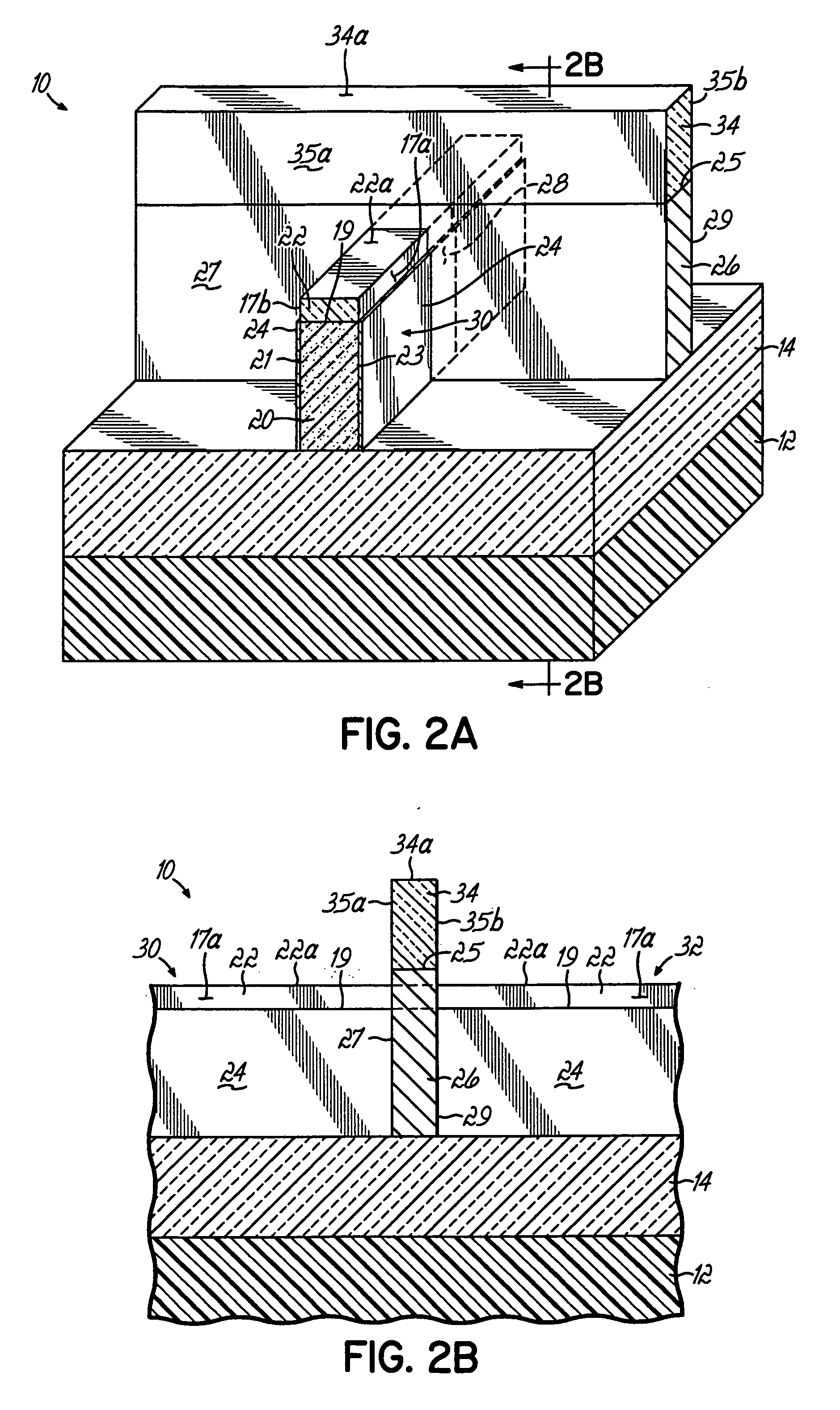
[0013] The present invention provides a semiconductor structure including fin-type field effect transistors (FinFET's) built on a semiconductor-on-insulator (SOI) wafer, as well as methods of making such semiconductor structures. Specifically, in one embodiment, the present invention is directed to semiconductor structure in which a dopant concentration may be introduced into the source / drain regions of a FinFET without affecting the dopant concentration of the gate electrode and methods of fabricating such semiconductor structures. The principles of the present invention may also be advantageous for forming interconnect metallization lines and the like. The present invention will now be described in greater detail by referring to the drawings that accompany the present application.
[0014] With reference to FIGS. 1A,B, a semiconductor wafer 10 comprises a semiconductor-on-insulator (SOI) substrate that includes a semiconductor substrate 12, which may be single crystal or monocrystal...
PUM
 Abstract
Description
Claims
Application Information
 - Generate Ideas
- Intellectual Property
- Life Sciences
- Materials
- Tech Scout
- Unparalleled Data Quality
- Higher Quality Content
- 60% Fewer Hallucinations
Browse by: Latest US Patents, China's latest patents, Technical Efficacy Thesaurus, Application Domain, Technology Topic, Popular Technical Reports.
© 2025 PatSnap. All rights reserved.Legal|Privacy policy|Modern Slavery Act Transparency Statement|Sitemap|About US| Contact US: help@patsnap.com