Method And Apparatus For Testing Particulate Contamination In Wafer Carriers

a technology of wafer carrier and wafer slurry, which is applied in the direction of cleaning hollow articles, cleaning using liquids, instruments, etc., can solve the problems of increasing the challenge of maintaining yield, increasing the difficulty of maintaining yield, and increasing the residual contamination within the foup, so as to avoid fm contamination

Inactive Publication Date: 2007-03-22
IBM CORP
View PDF12 Cites 42 Cited by
  • Summary
  • Abstract
  • Description
  • Claims
  • Application Information

AI Technical Summary

Benefits of technology

[0019] Another feature of the invention is that FM contamination can be avoided by purging with the gas flow.

Problems solved by technology

Contamination of an integrated circuit from particles deposited on the wafer during processing has always been a problem in the field of integrated circuit fabrication.
In addition, advanced technologies warrant larger die size, thus fewer particles can impact the same percentage of chips, causing an ever increasing challenge to maintain yields.
With such tight limits, the residual contamination within a FOUP becomes a significant factor affecting the yield.
When a FOUP has become excessively contaminated, it is sent out of the fab for a thorough (and expensive) cleaning process.
Further, an undetected contaminated FOUP will continue to contaminate wafers until it is detected.

Method used


Image

  • Method And Apparatus For Testing Particulate Contamination In Wafer Carriers
  • Method And Apparatus For Testing Particulate Contamination In Wafer Carriers
  • Method And Apparatus For Testing Particulate Contamination In Wafer Carriers

Examples


Embodiment Construction

[0026] A method of checking when a FOUP is contaminated according to the invention is an in-situ test for the residual contamination in the FOUP.

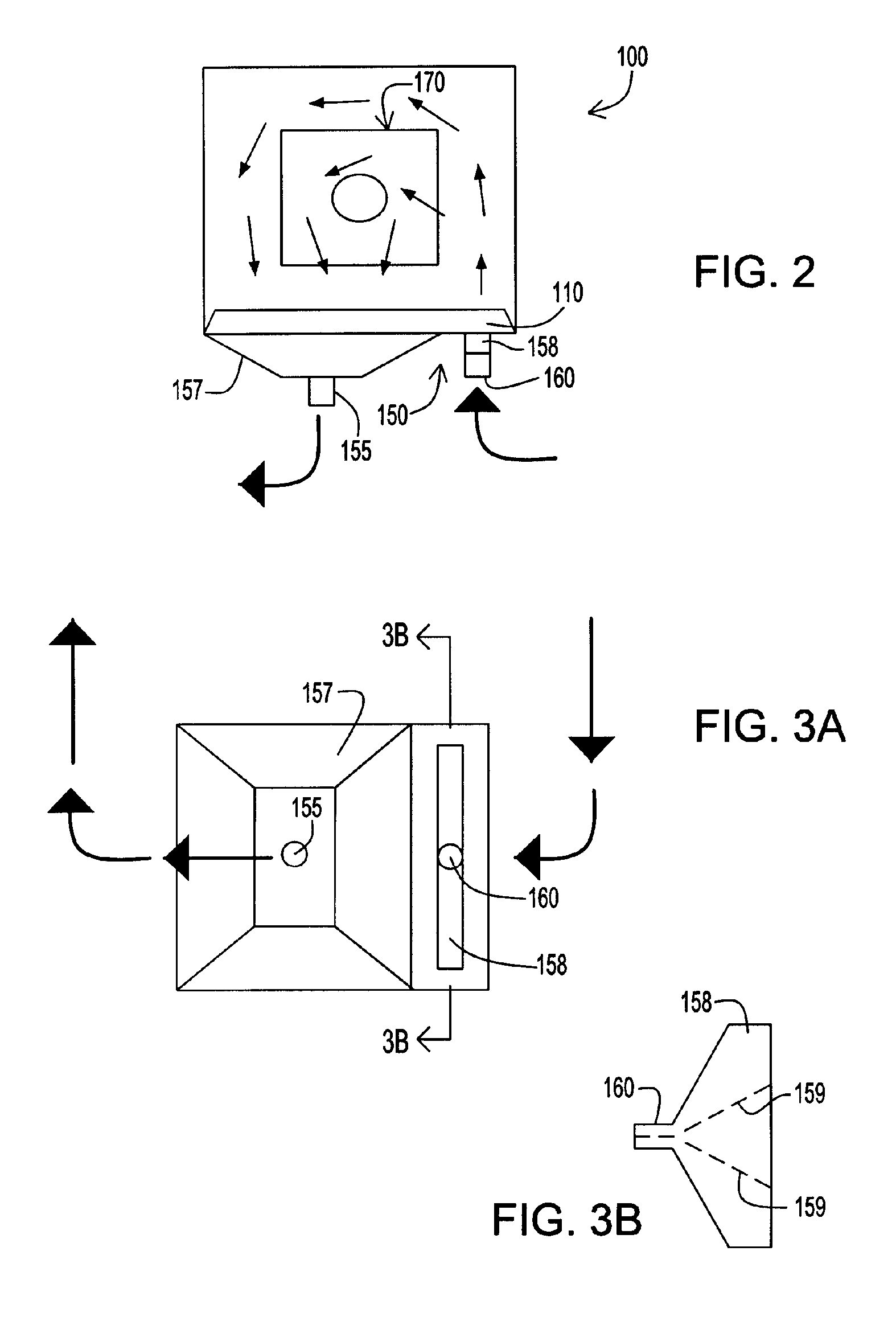
[0027] According to the invention, an in-situ test for residual contamination comprises flushing the FOUP with a gas such as nitrogen for a short time and measuring the number of particles that emerge.

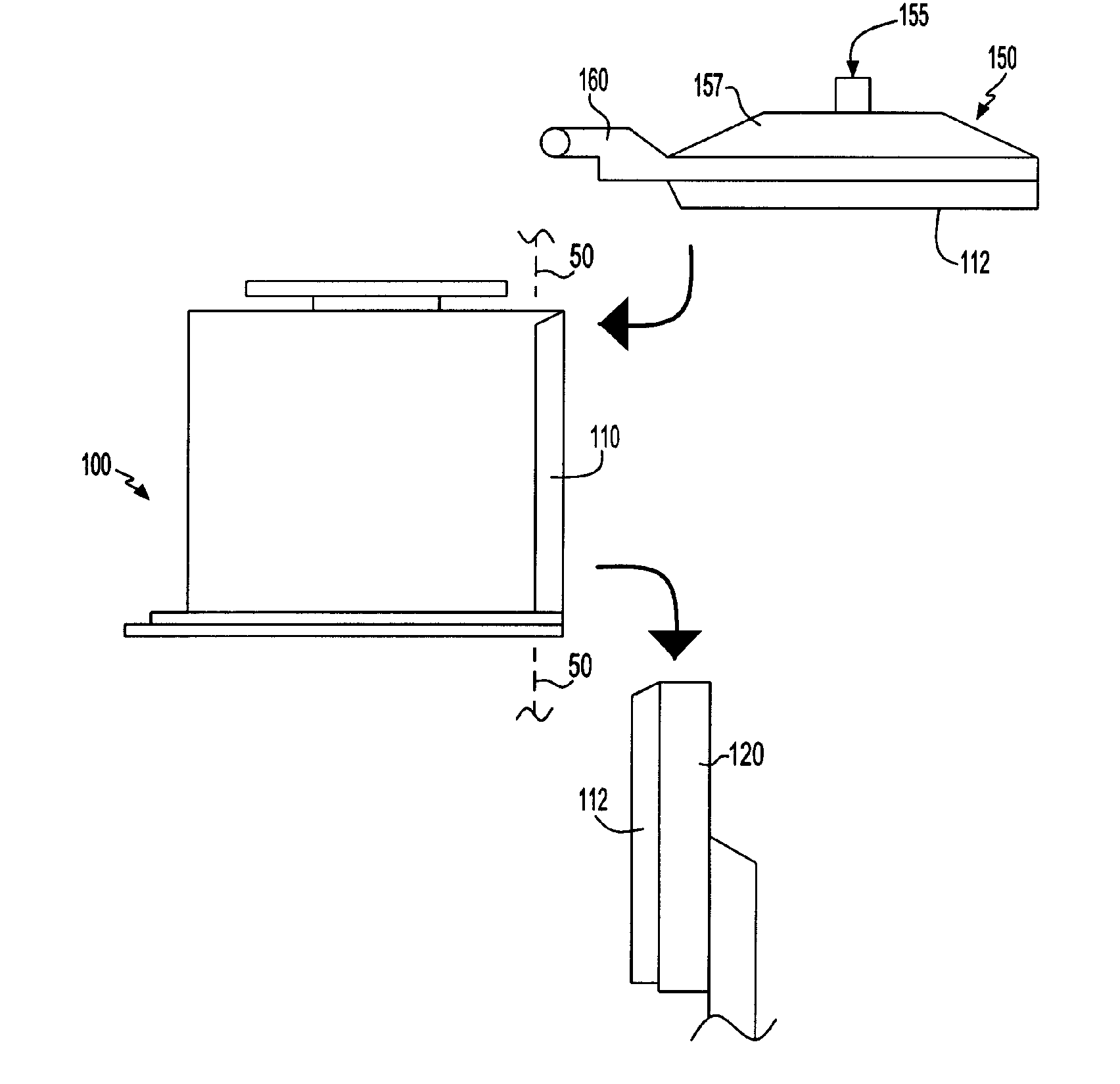
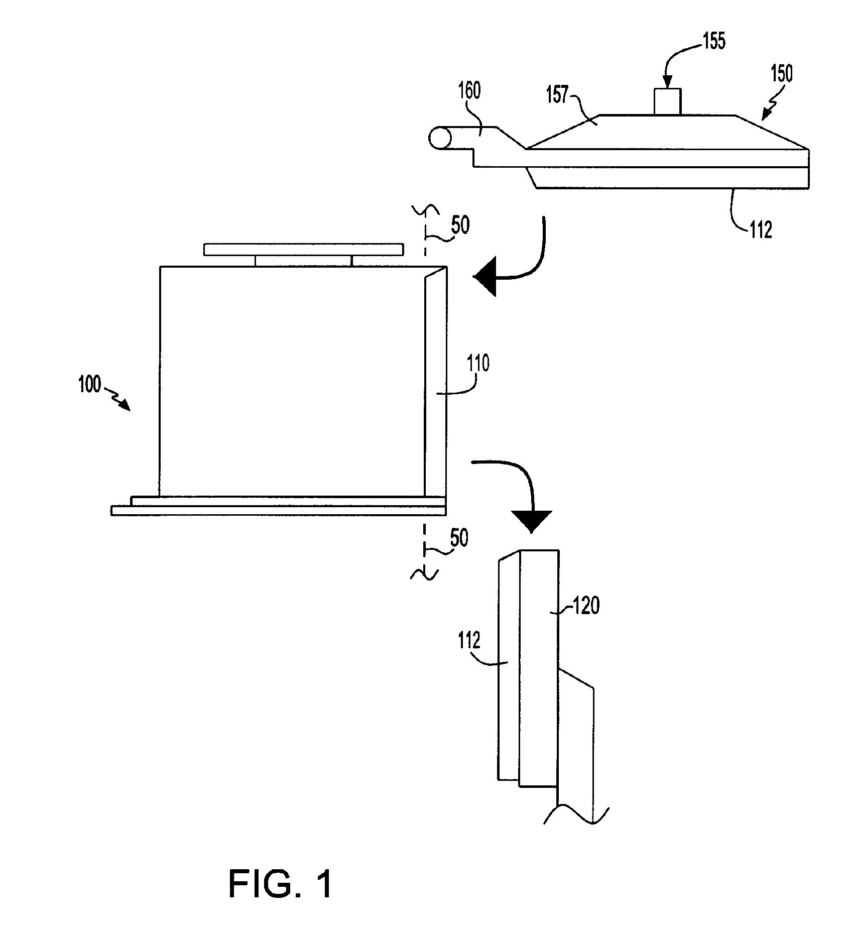
[0028]FIG. 1 shows a FOUP (100) loaded onto the port of a mapper / sorter (denoted schematically by dashed lines 50, with the FOUP enclosure's door (120) having been removed by the mapper / sorter's FOUP door opener and shown displaced and to the lower right of the Figure. This step exposes the internal surface of the FOUP to the mapper / sorter's internal environment. Once the FOUP door and door opener are clear of the FOUP opening, the face plate (112A) of the test cover 150 that is part of the Inspection System swings into place and seals against the FOUP door seal (110). The test cover is shown in the Figure as displaced from the FOUP and to t...


PUM


Abstract

Wafer carriers in an integrated circuit fab are tested for residual particle contamination by replacing the standard carrier door by a test cover having a gas inlet and outlet, counting the number of FM particles exiting the carrier during a flush cycle with a test gas having a known concentration of FM particles and either continuing processing if the number of FM particles is below a threshold, performing a purge with the test gas if the contamination is in a purge range, or sending the carrier out for cleaning if the number of FM particles is above the purge range.

Description

TECHNICAL FIELD [0001] The field of the invention is that of integrated circuit processing, in particular reduction of defects on a wafer by particles deposited on the wafer in the course of handling and transporting the wafers. BACKGROUND OF THE INVENTION [0002] Contamination of an integrated circuit from particles deposited on the wafer during processing has always been a problem in the field of integrated circuit fabrication. [0003] The limits on particulate contamination permitted in a clean room have been tightened with each generation of wafer size to an industry standard of 100 particles per cubic meter (@ 0.5 μm) in fabs using 200 mm wafers. [0004] With the advent of 300 mm wafers, the increased number of chips per wafer and the associated reduction in linewidth has required further reduction in permitted contamination levels. In addition, advanced technologies warrant larger die size, thus fewer particles can impact the same percentage of chips, causing an ever increasing c...

Claims


Application Information

Patent Timeline
Patent Type & Authority Applications(United States)
IPC IPC(8): B08B3/04
CPCG01N1/2202G01N15/06H01L21/67017H01L21/67389H01L21/67253H01L21/67288H01L21/67393H01L21/67028
Inventor KOCH, ROBERT T.MAYER, SOMER D.STEVENS, BRIANTOMASI, DEAN J.
Owner IBM CORP
Why Eureka
Try Eureka