Nonvolatile polymer bistability memory device using nano particles that are formed in polymer thin film and method of manufacturing the nonvolatile polymer bistability memory device

Inactive Publication Date: 2007-03-22
SAMSUNG ELECTRONICS CO LTD +1
View PDF1 Cites 9 Cited by
  • Summary
  • Abstract
  • Description
  • Claims
  • Application Information

AI Technical Summary

Problems solved by technology

Accordingly, the manufacturing process of the conventional flash memory device is difficult and complicated.
However, since conductive organic monomers are highly sensitive to moisture and heat, memory devices using conduc

Method used


Image

  • Nonvolatile polymer bistability memory device using nano particles that are formed in polymer thin film and method of manufacturing the nonvolatile polymer bistability memory device
  • Nonvolatile polymer bistability memory device using nano particles that are formed in polymer thin film and method of manufacturing the nonvolatile polymer bistability memory device
  • Nonvolatile polymer bistability memory device using nano particles that are formed in polymer thin film and method of manufacturing the nonvolatile polymer bistability memory device

Examples


Embodiment Construction

[0034] The present invention will now be described more fully with reference to the accompanying drawings, in which exemplary embodiments of the invention are shown. The invention may, however, be embodied in many different forms and should not be construed as being limited to the embodiments set forth herein; rather, these embodiments are provided so that this disclosure will be thorough and complete, and will fully convey the concept of the invention to those skilled in the art. Like reference numerals in the drawings denote like elements, and thus their description will be omitted.

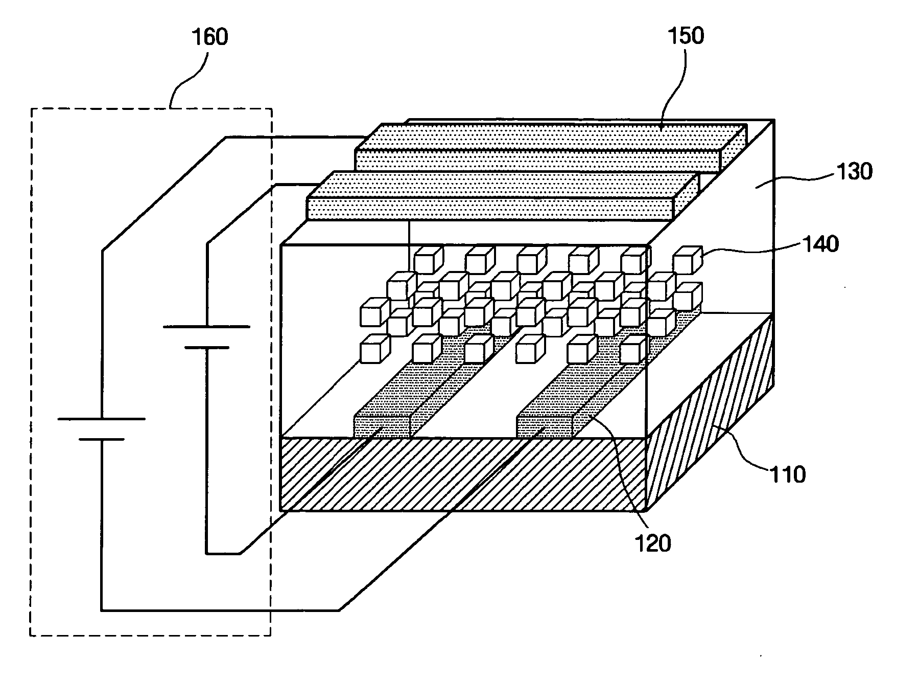
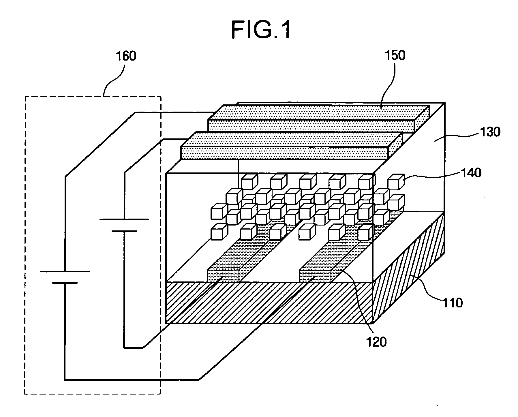
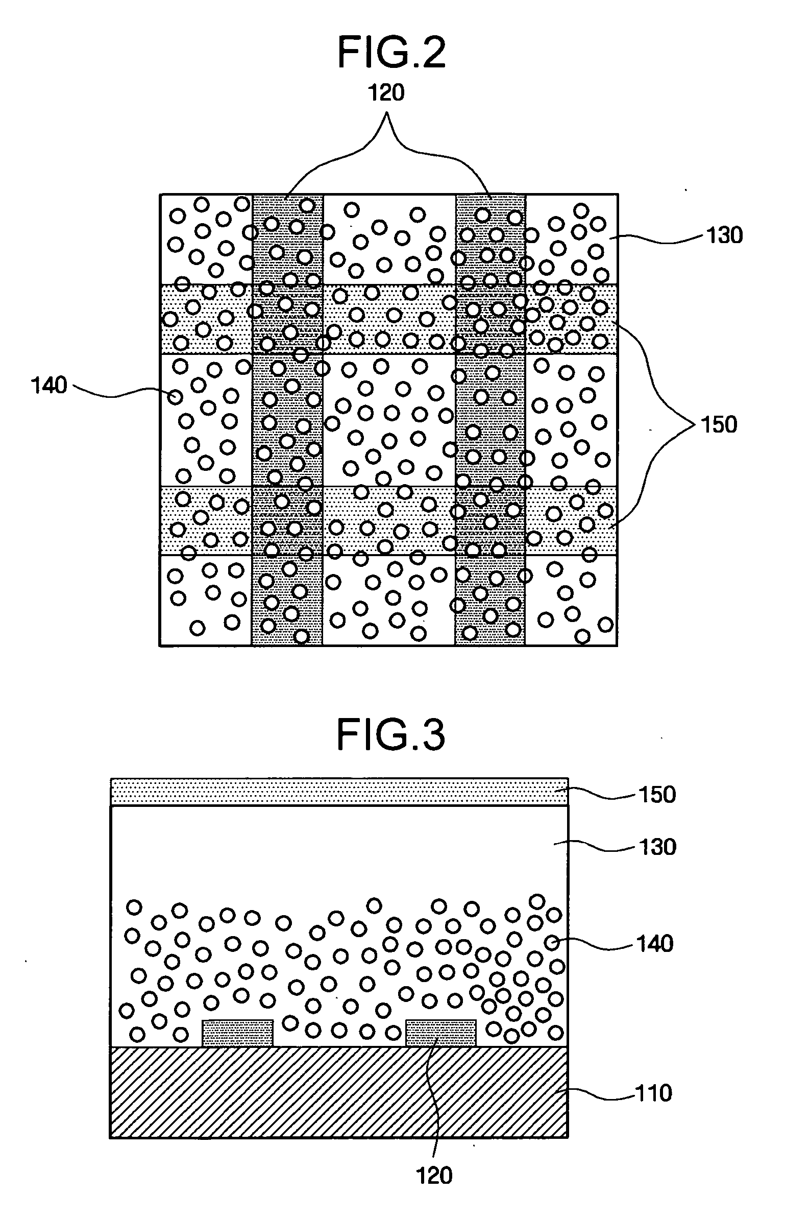
[0035]FIG. 1 is a perspective view of a nonvolatile polymer bistability memory device using nano particles that are formed in a polymer thin film, according to an exemplary embodiment of the present invention, FIG. 2 is a plan view of the nonvolatile polymer bistability memory device illustrated in FIG. 1, and FIG. 3 is a cross-sectional view of the nonvolatile polymer bistability memory device illustr...


PUM

PropertyMeasurementUnit
Temperatureaaaaaaaaaa
Timeaaaaaaaaaa

Abstract

A nonvolatile polymer bistability memory device using nano particles that are formed in a polymer thin film and a method of manufacturing the nonvolatile polymer bistability memory device are provided. The nonvolatile polymer bistability memory device includes a semiconductor substrate, a first electrode on the semiconductor substrate, a polymer thin film on the first electrode, nano particles embedded into the polymer thin film, and a second electrode on the polymer thin film. The nonvolatile polymer bistability memory device does not need any source and drain to operate, and the method of manufacturing the nonvolatile polymer bistability memory device can guarantee high production efficiencies while maintaining low manufacturing costs.

Description

BACKGROUND OF THE INVENTION [0001] 1. Field of the Invention [0002] The present invention relates to a semiconductor memory device, and more particularly, to a nonvolatile polymer bistability memory device using nano particles embedded in a polymer thin film, and a method of manufacturing the nonvolatile polymer bistability memory device. [0003] This application claims priority from Korean Patent Application No. 10-2005-0086530 filed on Sep. 15, 2005 in the Korean Intellectual Property Office, the disclosure of which is incorporated herein by reference in its entirety. [0004] 2. Description of the Related Art [0005] Nonvolatile memory devices do not lose data stored therein even when power supply is interrupted. Flash memory devices, which are one of the most representative nonvolatile memory devices, comprise a plurality of unit cells, each unit cell having an electrically isolated floating gate. Data stored in each unit cell of a flash memory device may be classified into data hav...

Claims


Application Information

Patent Timeline
IPC IPC(8): G02F1/1333
CPCB82Y10/00G11C13/0014G11C13/0016G11C2213/77H01L27/285H01L27/2472H01L51/0035H01L45/10H01L45/1233H01L45/14H01L45/1608H01L27/286H10B63/82H10N70/25H10N70/826H10N70/881H10N70/021H10K19/20H10K19/202H10K85/111H10N70/20
Inventor KIM, TAE-WHANKIM, YOUNG-HOKIMJUNG, JEA-HUN
Owner SAMSUNG ELECTRONICS CO LTD
Why Eureka
Try Eureka