Wafer packing

Inactive Publication Date: 2007-03-29
UNITED MICROELECTRONICS CORP
View PDF10 Cites 10 Cited by
  • Summary
  • Abstract
  • Description
  • Claims
  • Application Information

AI Technical Summary

Benefits of technology

[0010] The present invention utilizes hollow support pads inserted between each wafer in the wafer packing, in order to separate stacked wafers. The present invention can avoid the pollution and scraping of the waf

Problems solved by technology

The manufacturing of semiconductor wafers includes many complex processes.
As above-mentioned, in order to avoid interleafs polluting wafers,

Method used


Image

  • Wafer packing
  • Wafer packing
  • Wafer packing

Examples


Example

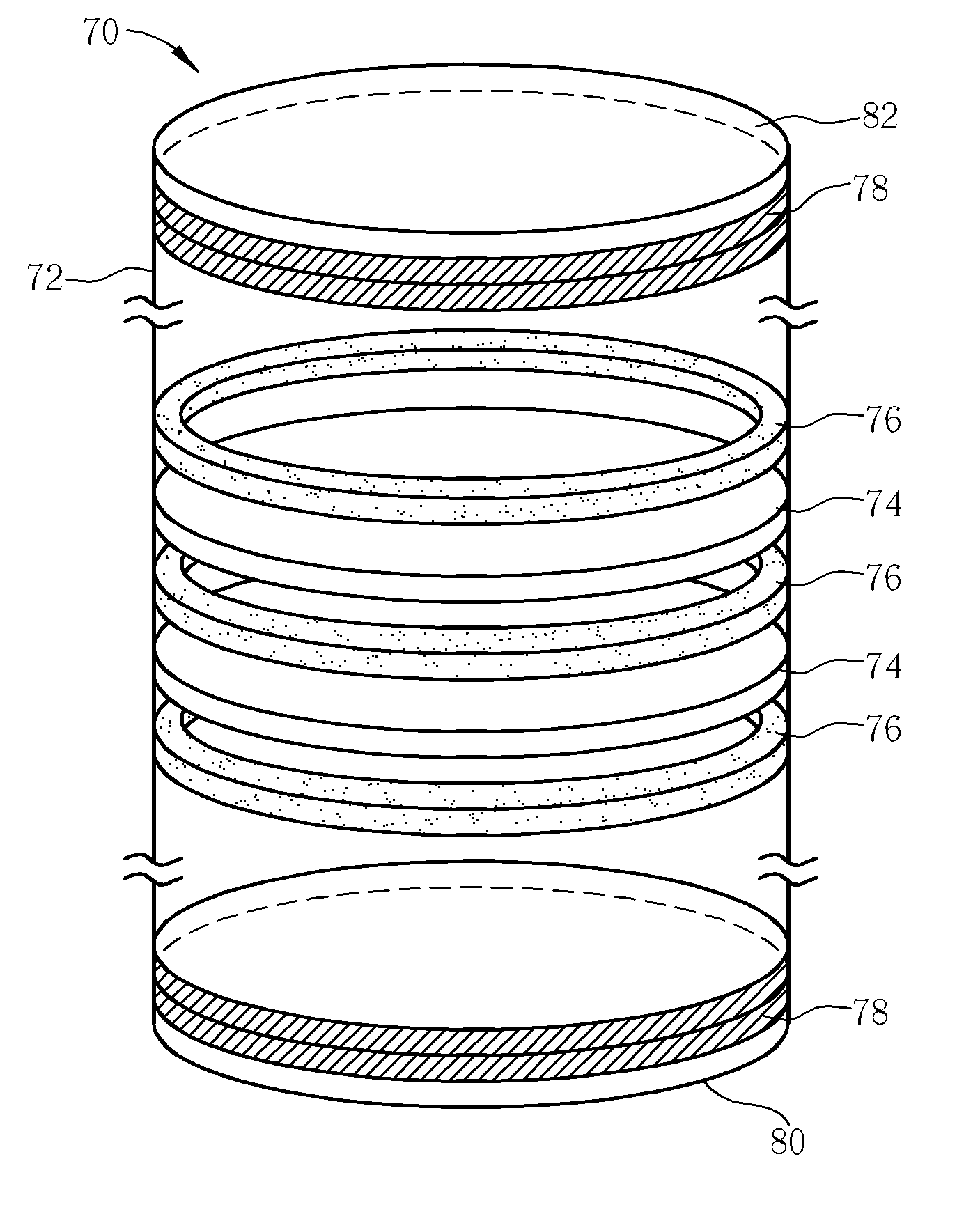
[0015] Please refer to FIG. 4 that is a schematic diagram of a wafer packing 70 according to the present invention. The wafer packing 70 includes a cassette 72, at least two sponges 78, and a plurality of hollow support pads 76 for depositing a plurality of wafers 74. First, at least one of the sponges 78 is put on a bottom of the cassette 72, and at least one hollow support pad 76 and a wafer 74 are alternately put on the sponges 78. Other hollow support pads 76 and other wafers 74 are continuously and repeatedly stacked in alternation on the bottom wafer 74 until the cassette is filled with 25 wafers 74, although this quantity is not limiting as other quantities are equally possible. Then, a lid 82 of the cassette 72 covers and completes the batch of wafer packing 70. A quantity of wafer packings 70 is stored in a carton (not shown) for shipment. In addition, the hollow support pads 76 touch a non-complete wafer area of the wafers 74, so the complete wafer area of the wafers 74 ca...


PUM


Abstract

The present invention provides a wafer packing. The wafer packing includes a box, at least two sponges, at least two hollow support pads, and a plurality of wafers. The sponges are put on a bottom and under a lid of the box, the hollow support pads are put between sponges, and each wafer is put between adjacent hollow support pads touching a non-complete wafer area of each wafer.

Description

BACKGROUND OF THE INVENTION [0001] 1. Field of the Invention [0002] The invention relates to wafer packing, and more particularly, to wafer packing that avoids wafer pollution and saves space. [0003] 2. Description of the Prior Art [0004] The manufacturing of semiconductor wafers includes many complex processes. Processes for forming transistors or other devices on semiconductor wafers and processes for packaging wafers are usually undertaken by different manufacturers, or performed in different factories. When a wafer manufacturer ships the wafers to a packager, the wafers are stored in cartons or wafer transfer apparatuses, for delivery to the packager. [0005] Please refer to FIG. 1 that is schematic diagram of wafer packing according to prior art. A wafer packing 10 includes a cassette 12 for depositing a plurality of wafers 14, and utilizes a interleaf 16 between adjacent wafers 14 for separating the wafers 14. The function of the interleaf 16 is to prevent damage to the wafers ...

Claims


Application Information

Patent Timeline
IPC IPC(8): B65D85/00
CPCH01L21/67383
Inventor HSIAO, HUANG-TING
Owner UNITED MICROELECTRONICS CORP
Why Eureka
Try Eureka