This helps you quickly interpret patents by identifying the three key elements:
Problems solved by technology
Method used
Benefits of technology
Benefits of technology
[0076] To briefly explain the advantageous effects obtained by the typical inventions among the inventions disclosed in this specification, they are as follows.
[0077] According to the display device of the present invention which incorporates the touch panel function therein, it is possible to reduce the number of elements which constitutes the photo sensor circuit and it is also possible to detect the accurate input coordinate position without requiring the particular coordinate arithmetic circuit.
[0078] Hereinafter, an embodiment in which the present invention is applied to the liquid crystal display device is explained in detail in conjunction with attached drawings.
[0079] Here, in all drawings for explaining the embodiments, parts having identical functions are given same numerals and their repeated explanation is omitted.
Problems solved by technology
Accordingly, the conventional touch panel has drawbacks such that the visibility is deteriorated due to the increase of surface reflection, a mechanism which mounts the touch panel on the display becomes necessary, and a means which calibrates an output of the touch panel and a position of a display becomes necessary.
Method used
Image
Click on the blue label to locate the original text in one second.
Reading with bidirectional positioning of images and text.
Examples
embodiment 1
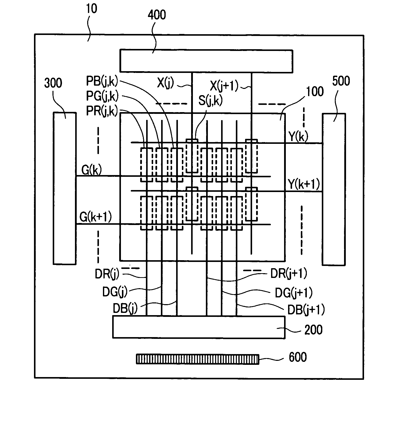
[0097]FIG. 1 is a block diagram showing the constitution of a liquid crystal display panel of a liquid crystal display device according to an embodiment 1 of the present invention.
[0098] The liquid crystal display panel of the embodiment incorporates a photo sensor circuit (a photo detection circuit) therein.
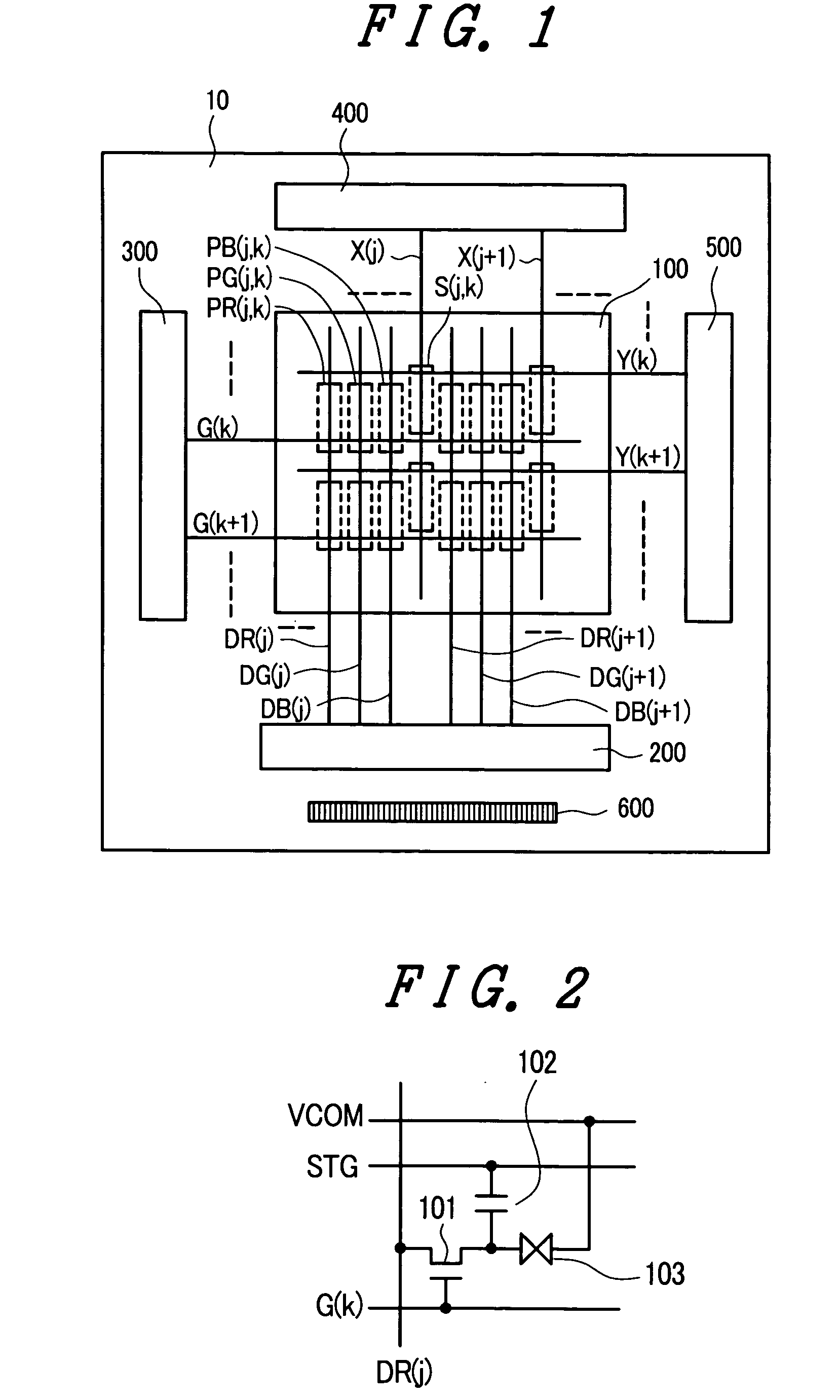
[0099] The liquid crystal display panel 10 of this embodiment includes a display part 100 and is constituted of a drain drive circuit 200, a gate drive circuit 300, an X output circuit 400, a Y output circuit 500, and terminals 600.
[0100] The display part 100 includes sub pixels PR(j,k), PG(j,k), PB(j,k) having color filters corresponding to three primary colors respectively and photo sensor circuits S(j,k) which are arranged in a matrix array. One pixel is constituted of three sub pixels (PR(j,k), PG(j,k) , PB(j,k).
[0101] A gate line G(k) which is outputted from the gate drive circuit 300 and drain lines (DR(j), DG(j), DB(j)) which are outputted from the drain drive circuit...
embodiment 2
[0167] A liquid crystal display panel of a liquid crystal display device according to an embodiment 2 of the present invention also incorporates a photo sensor circuit therein.
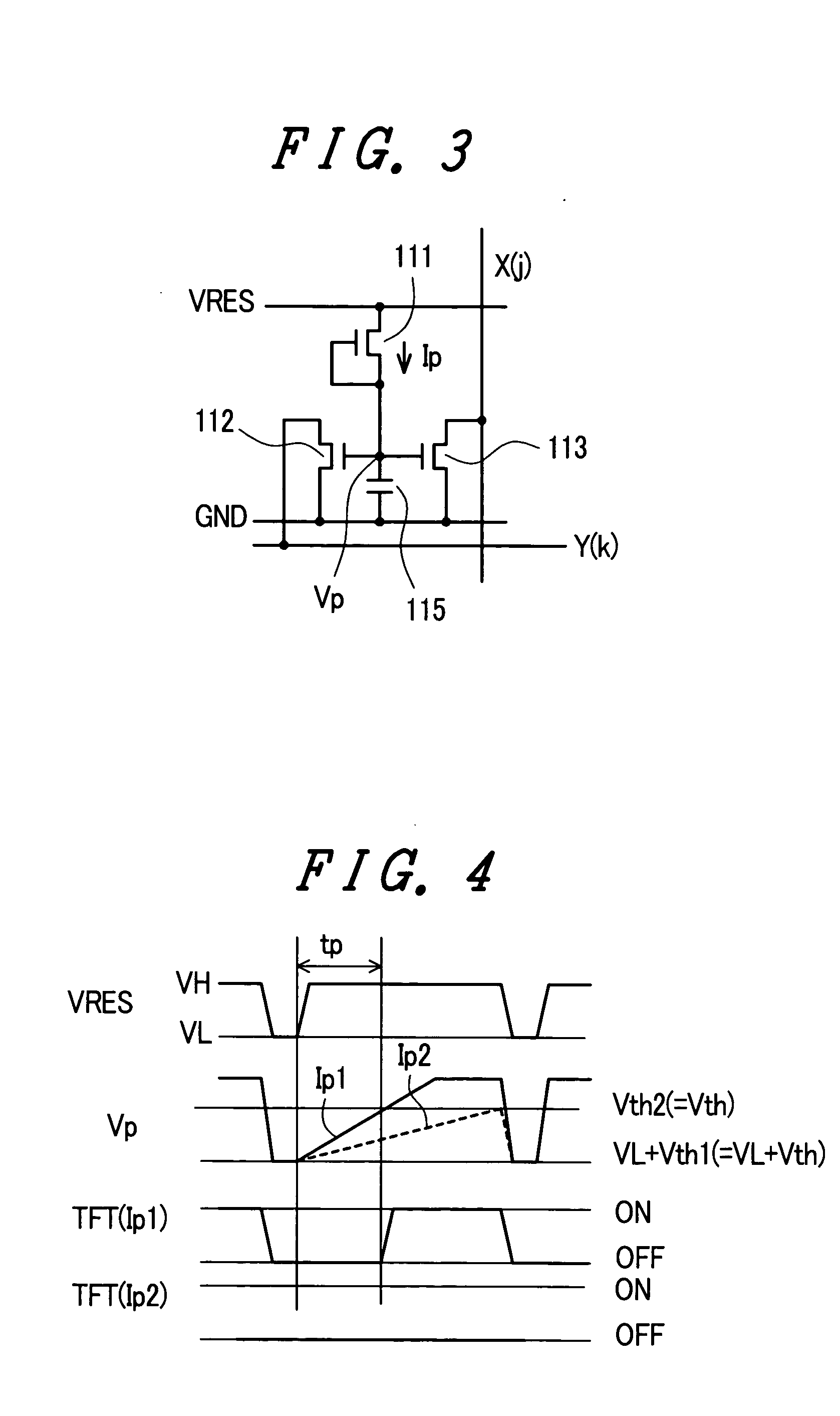
[0168]FIG. 9 is a circuit diagram showing an equivalent circuit of an example of a photo sensor circuit S(j,k) according to the embodiment.
[0169] As shown in the drawings, the photo sensor circuit S(j,k) according to this embodiment is constituted of a photodiode 121, TFTs (122, 123) and a bootstrap capacitance (hereinafter referred to as BS capacitance) 124.
[0170] The photo diode 121 has one end thereof connected to a gate line Vg(k+1) of a next stage and has another end connected to a gate of the TFT 122. The BS capacitance is connected between a gate and a drain of the TFT 122.
[0171] Further, a source of the TFT 122 and a gate of the TFT 123 are connected to the own-row gate line Vg(k), a source of the TFT 123 is connected to the drain of the TFT 122, and a drain of the TFT 123 is connected to X output ...
embodiment 3
[0181] A liquid crystal display panel of a liquid crystal display device according to the embodiment 3 of the present invention also incorporates a photo sensor circuit therein.
[0182]FIG. 11 is a circuit diagram showing an equivalent circuit of one example of the photo sensor circuit S(j,k) of this embodiment.
[0183] The photo sensor circuit S(j,k) of this embodiment differs from the above-mentioned photo sensor circuit S(j,k) of the embodiment 2 with respect to a point that a PN junction of the photo diode 121 is inverted and a point that one end of the photo diode 121 is connected to an initializing control line Vdsc(k+1).
[0184]FIG. 12 is a timing chart for explaining the operation of the photo sensor circuit S(j,k) shown in FIG. 11.
[0185] The voltage Vdsc(k+1) of the initializing control line is a signal which has a phase opposite to a phase of the voltage Vg(k+1) of the gate line, wherein when the voltage Vdsc(k+1) is at the L level, the photo diode 121 assumes the normal bia...
PUM
Abstract
A display device which incorporates a touch panel function therein can reduce the number of elements which constitute a photo sensor circuit and can accurately detect an input coordinate position without requiring a particular coordinate arithmetic circuit. In a display device which includes: a display part on which a plurality of pixels are arranged in a matrix array; and a plurality of photo detection circuits which are arranged in a matrix array in the inside of the display part, each photo detection circuit of the plurality of photo detection circuits includes: a photo sensor which converts an incident light into a optical current corresponding to intensity of the incident light; an integral capacitance which integrates the optical current converted by the photo sensor; and a comparator to which a voltage of the integral capacitance is inputted; and the comparator includes a transistor of an open drain output type with a grounded source.
Description
CROSS-REFERENCE TO RELATED APPLICATIONS [0001] The disclosure of Japanese Patent Application No. P2005-281061 filed on Aug. 29, 2005 including the claims, the specification, the drawings and the abstract is incorporated herein by reference in its entirety. BACKGROUND [0002] 1. Field of the Invention [0003] The present invention relates to a display device, and more particularly to a display device which includes a touch panel function. [0004] 2. Description of Related Art [0005] As a display device which includes a coordinates inputting device, there has been known a display device which includes a touch panel. [0006] The conventional touch panel is mainly of a resistance film type and adopts the structure which mounts the touch panel on the display panel. Accordingly, the conventional touch panel has drawbacks such that the visibility is deteriorated due to the increase of surface reflection, a mechanism which mounts the touch panel on the display becomes necessary, and a means whi...
Claims
Application Information
Patent Timeline
Application Date:The date an application was filed.
Publication Date:The date a patent or application was officially published.
First Publication Date:The earliest publication date of a patent with the same application number.
Issue Date:Publication date of the patent grant document.
PCT Entry Date:The Entry date of PCT National Phase.
Estimated Expiry Date:The statutory expiry date of a patent right according to the Patent Law, and it is the longest term of protection that the patent right can achieve without the termination of the patent right due to other reasons(Term extension factor has been taken into account ).
Invalid Date:Actual expiry date is based on effective date or publication date of legal transaction data of invalid patent.

