

Ferroelectric film with ferroelectric domain array and method for forming same
- Summary
- Abstract
- Description
- Claims
- Application Information
AI Technical Summary
Benefits of technology
Problems solved by technology
Method used
Image

Examples
Embodiment Construction
[0018] Reference will now be made to the drawings to describe preferred embodiments of the present ferroelectric film with ferroelectric domain array and method for forming the same in detail.
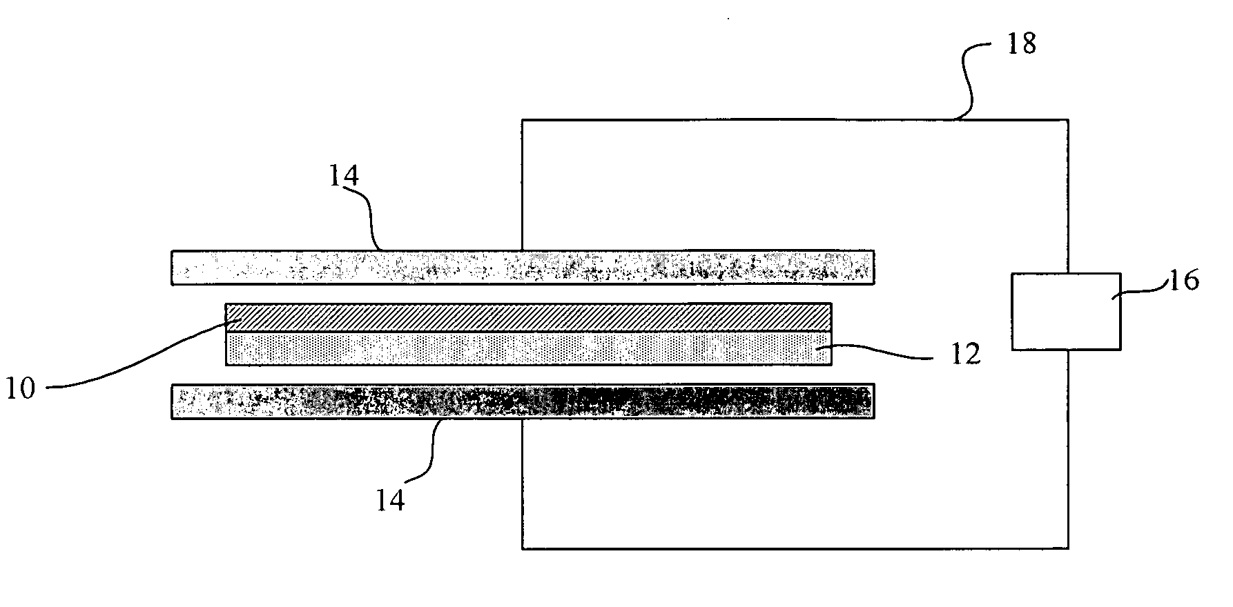
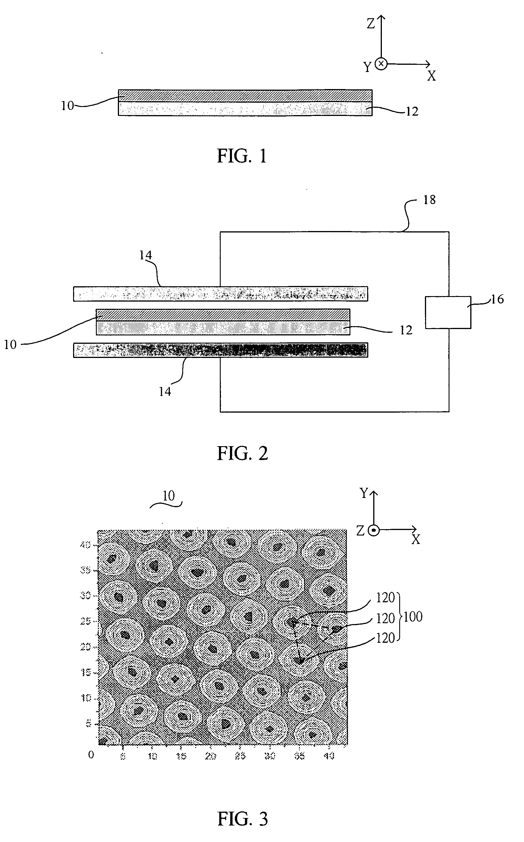
[0019] FIGS. 1 to 3 illustrate successive stages in a process for forming a ferroelectric film with an array of ferroelectric nanodomains in accordance with a preferred embodiment.
[0020] Referring to FIG. 1, a ferroelectric film 10 formed on a substrate 12 is provided. The ferroelectric film 10 has a quasi 2-dimensional configuration, and is comprised of a ferroelectric material. The ferroelectric film 10 generally comprises a plurality of unit cells. Advantageously, in a rectangular coordinate system, the ferroelectric film 10 has a thickness in the range from about 2 to 100 unit cells along the Z axis direction, where the Z axis direction is a direction that is normal to the ferroelectric film 10; and atoms constituting the ferroelectric film 10 are periodical distribution along the X and Y...
PUM
| Property | Measurement | Unit |
|---|---|---|
| Diameter | aaaaa | aaaaa |
| Electric field | aaaaa | aaaaa |
| Thickness | aaaaa | aaaaa |
Abstract
Description
Claims
Application Information