MOS transistor and manufacturing method thereof

Inactive Publication Date: 2007-03-29
DONGBU ELECTRONICS CO LTD
View PDF3 Cites 3 Cited by
  • Summary
  • Abstract
  • Description
  • Claims
  • Application Information

AI Technical Summary

Benefits of technology

[0012] Another object of the present invention is to provide a method of forming a MOS transistor, in which a nickel salicide layer is formed using silicon carbide so that the MOS transistor has low resistance contact characteristics.
[0013] Still another object of the present invention is to provide a MOS transistor capable of having low resistance contact characteristics while improving a drive current thereof by forming a modified silicon channel and a nickel salicide layer, using silicon carbide.

Problems solved by technology

However, such a silicon epitaxial layer may cause lattice damage to silicon, thereby increasing leakage current of the MOS transistor.
However, this method may increase the manufacturing cost due to the addition of a nitride layer depositing process.
However, surface resistance of the thin polycrystalline silicon gate and the source-drain active region, which are prepared corresponding to the scale-down of the semiconductor device, generally are not reduced to a level below a range between 10 to 20 ohms / square.
However, the nickel salicide layer obtained through the above nickel salicide process is generally thermally unstable at a temperature of 500° C. or above, which corresponds to the temperature of a chemical vapor deposition process for forming a subsequent (e.g., inter-metal) layer, which may cause contact leakage current.
However, this method introduces an additional manufacturing cost.

Method used


Image

  • MOS transistor and manufacturing method thereof
  • MOS transistor and manufacturing method thereof
  • MOS transistor and manufacturing method thereof

Examples


Embodiment Construction

[0017] Hereinafter, a preferred embodiment according to the present invention will be described in detail, with reference to the following drawings.

[0018] In the following description of the present invention, technologies which are generally known in the art and do not directly relate to the present invention will be omitted in order to avoid redundancy and to clarify the subject manner of the present invention. In the same manner, some of elements are exaggerated, omitted or simplified in the drawings and the elements may have sizes different from those shown in drawings, in practice.

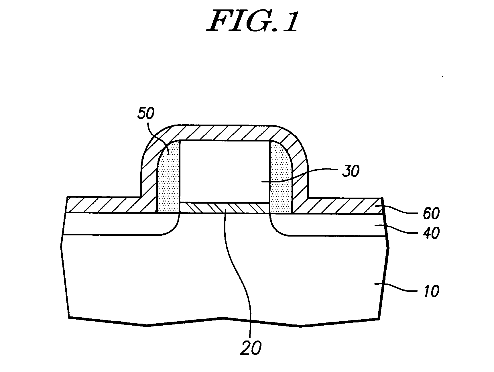
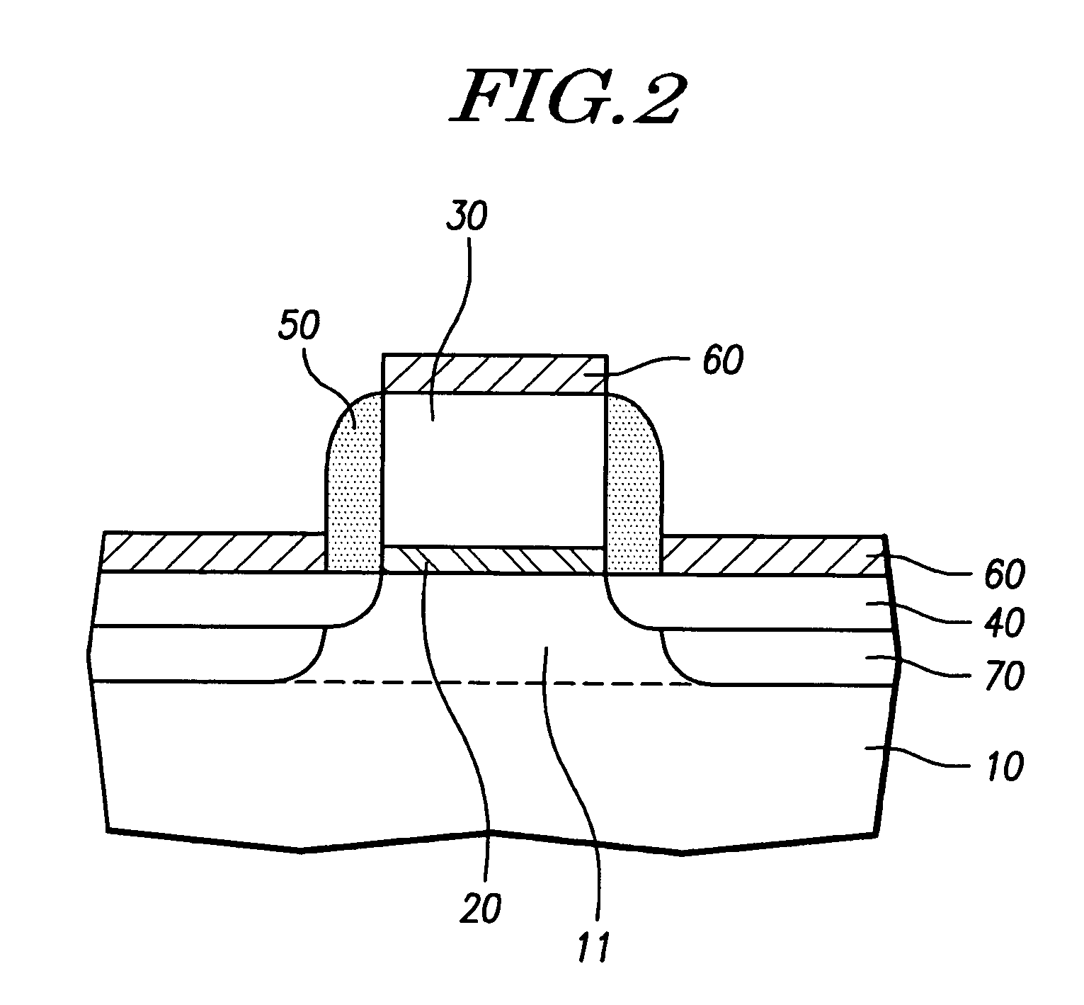
[0019] FIGS. 1 to 3 are views illustrating a method of manufacturing a MOS transistor according to the preferred embodiment of the present invention.

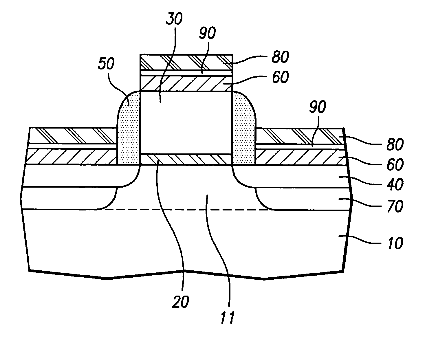
[0020] First, prior to forming silicon carbide on a semiconductor device according to the present invention, a gate oxide layer 20, a gate 30, a lightly doped drain (LDD) 40 and a spacer 50 are formed on a silicon substrate 10 as shown in FIG. 1.

[0021...


PUM

PropertyMeasurementUnit
Temperatureaaaaaaaaaa
Lattice constantaaaaaaaaaa
Structureaaaaaaaaaa

Abstract

Disclosed are a MOS transistor having a low resistance ohmic contact characteristic and a manufacturing method thereof capable of improving a drive current of the MOS transistor. A gate oxide layer, a gate electrode, and a spacer are formed on a silicon substrate, and a silicon carbide layer is deposited thereon. A photolithography process is performed, and the silicon carbide layer is etched except for predetermined portions corresponding to source-drain regions and the gate electrode. Then, a metal layer is formed on the resulting structure after performing a source-drain ion implantation process. The metal layer is heated to form a salicide layer on the gate electrode and the source-drain diffusion regions. Then, the unreacted metal layer is removed, thereby forming the MOS transistor.

Description

[0001] This application claims the benefit of Korean Application No. 10-2005-0088661, filed on Sep. 23, 2005, which is incorporated by reference herein in its entirety. BACKGROUND OF THE INVENTION [0002] 1. Field of the Invention [0003] The present invention relates to a MOS transistor and a manufacturing method thereof, and more specifically, to a MOS transistor and a manufacturing method thereof, in which a modified silicon channel is formed using silicon carbide, thereby improving a drive current of the MOS transistor, and in which a nickel salicide layer may be formed using silicon carbide so that the MOS transistor has low resistance contact characteristics. [0004] 2. Background of the Related Art [0005] With the rapid development of high-speed and high-integration semiconductor devices, micro-sized transistors have been realized. As the semiconductor devices have become highly integrated, a drive current of the semiconductor device may be reduced, so that the performance of th...

Claims


Application Information

Patent Timeline
IPC IPC(8): H01L21/336H01L21/4763
CPCH01L21/28518H01L29/41783H01L29/7843H01L29/6659H01L29/7834H01L29/665H01L21/18
Inventor PARK, HYUK
Owner DONGBU ELECTRONICS CO LTD
Why Eureka
Try Eureka