Multi-port memory device

a memory device and multi-port technology, applied in the field of multi-port memory devices, can solve the problems of reducing the efficiency of utilization to the density of the whole memory device, difficult to detect whether the write command is applied or not, and difficulty in implementing various multimedia functions

Active Publication Date: 2007-03-29
SK HYNIX INC
View PDF2 Cites 14 Cited by
  • Summary
  • Abstract
  • Description
  • Claims
  • Application Information

AI Technical Summary

Benefits of technology

[0025] In accordance with an aspect of the present invention, there is provided a multi-port memory device having a plurality of ports performing a serial input/output (I/O) communication with external devices, and a plurality of banks performing a parallel I/O communication with the ports through a plurality of global I/O lines, the multi-port memory device including: a write clock generating unit for generating a write clock which is selectively toggled only while write data are applied; a write control unit for generating a write flag signal group and a write driver enable signal in response to the write clock and a write command; a data latch unit for outputting intermediate write data by storing burst write data under the control of the write flag signal group; and a write driver for receiving the intermediate write data output from the data latch unit to write final write data to a memory cell of a corresponding bank in response to the write driver enable signal and a data mask signal group.
[0026] In accordance with a further aspect of the present invention, there is provided...

Problems solved by technology

However, in the single port memory device, it is difficult to implement various multimedia functions because the single port memory device uses only one port.
When the DRAM devices are constituted independent of each other, it is difficult to allocate a proper memory amount between memory devices based on the number of access times. As a result, an efficiency of u...

Method used


Image

  • Multi-port memory device
  • Multi-port memory device
  • Multi-port memory device

Examples


Embodiment Construction

[0044] Hereinafter, a multi-port memory device with a serial input / output (I / O) interface in accordance with exemplary embodiments of the present invention will be described in detail with reference to the accompanying drawings.

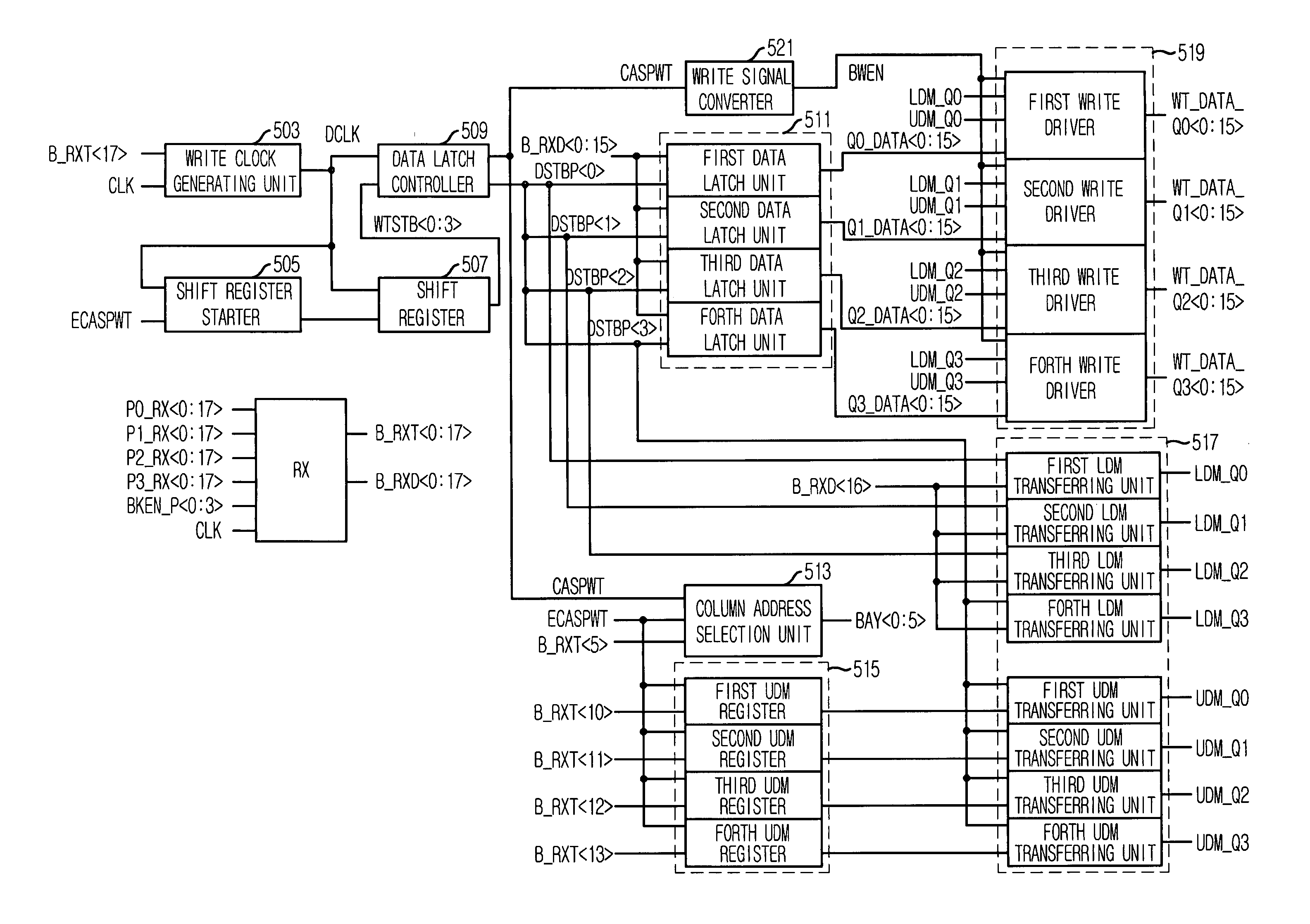
[0045]FIG. 5 is a block diagram of a bank controller provided in a multi-port memory device relating to a write operation path in accordance with an embodiment of the present invention. Herein, the write operation path corresponds to one of a plurality of banks. If the number of banks is eight, the multi-port memory device includes eight write operation paths.

[0046] The write operation path includes a receiver (RX) 501, a write clock generating unit 503, a write control unit 505, 507, 509, and 521, a data latch unit 511, a column address selection unit 513, a write data mask signal storage unit 515 and 517, and a write driver 519.

[0047] The RX 501 generates a burst write command B_RXT0:17> and a burst write data B_RXD0:17> by selecting one of parallel data...


PUM


Abstract

A multi-port memory device having a plurality of ports performing a serial input/output (I/O) communication with external devices, and a plurality of banks performing a parallel I/O communication with the ports through a plurality of global I/O lines. The multi-port memory device includes: a write clock generating unit for generating a write clock selectively toggled only while write data are applied; a write control unit for generating a write flag signal group and a write driver enable signal in response to the write clock and a write command; a data latch unit for outputting intermediate write data by storing burst write data under the control of the write flag signal group; and a write driver for receiving the intermediate write data to write final write data in a memory cell of a corresponding bank in response to the write driver enable signal and a data mask signal group.

Description

FIELD OF THE INVENTION [0001] The present invention relates to a multi-port memory device, and more particularly, to a bank control logic unit of a multi-port memory device for supporting a preemption burst write operation and an interrupt write operation as well as a normal write operation. DESCRIPTION OF RELATED ARTS [0002] Currently, most dynamic random access memory (DRAM) are used in a high definition television (HDTV) and a liquid crystal display (LCD) TV as well as traditional devices such as a desktop computer, a notebook computer and a server. Accordingly, there is a demand for a new data communication instead of a conventional data communication having a single port with a plurality of input / output (I / O) pin sets, i.e., a parallel I / O interface. [0003]FIG. 1 is a block diagram of a conventional single port memory device. For convenience of explanation, a conventional x16 512M DRAM device having eight banks as the single port memory device is illustrated. [0004] The x16 512...

Claims


Application Information

Patent Timeline
IPC IPC(8): G06F12/00
CPCG11C7/1027G11C2207/108G11C7/1078G11C7/1087G11C7/1093G11C7/1096G11C7/22G11C7/222G11C8/12G11C8/16G11C11/4076G11C11/4087G11C11/4096G11C2207/107G11C7/1075G11C7/10G11C8/04
Inventor KIM, JAE-ILDO, CHANG-HO
Owner SK HYNIX INC
Why Eureka
Try Eureka