Antenna, radio device, method of designing antenna, and nethod of measuring operating frequency of antenna

a radio device and antenna technology, applied in the direction of resonant antennas, radiating element structural forms, antennas, etc., can solve the problem of complex design that is required, and achieve the effect of easy design

Active Publication Date: 2007-04-05
DENSO CORP
View PDF8 Cites 26 Cited by
  • Summary
  • Abstract
  • Description
  • Claims
  • Application Information

AI Technical Summary

Benefits of technology

[0009] The present invention therefore has an object to provide an antenna that has a wide frequency band and is easy to design, radio device, a method of designing the antenna, and a method of measuring the operating frequency of the antenna.

Problems solved by technology

However, when the size of the ground electrode of the patch antennas is small, the directivity of the antennas is insufficient for radiation in the front direction, so that some radio waves leak to sides and the rear, possibly resulting in interference.
Therefore, a complicated design is required to bring their resonance frequencies into agreement with each other.

Method used


Image

  • Antenna, radio device, method of designing antenna, and nethod of measuring operating frequency of antenna
  • Antenna, radio device, method of designing antenna, and nethod of measuring operating frequency of antenna
  • Antenna, radio device, method of designing antenna, and nethod of measuring operating frequency of antenna

Examples


first embodiment

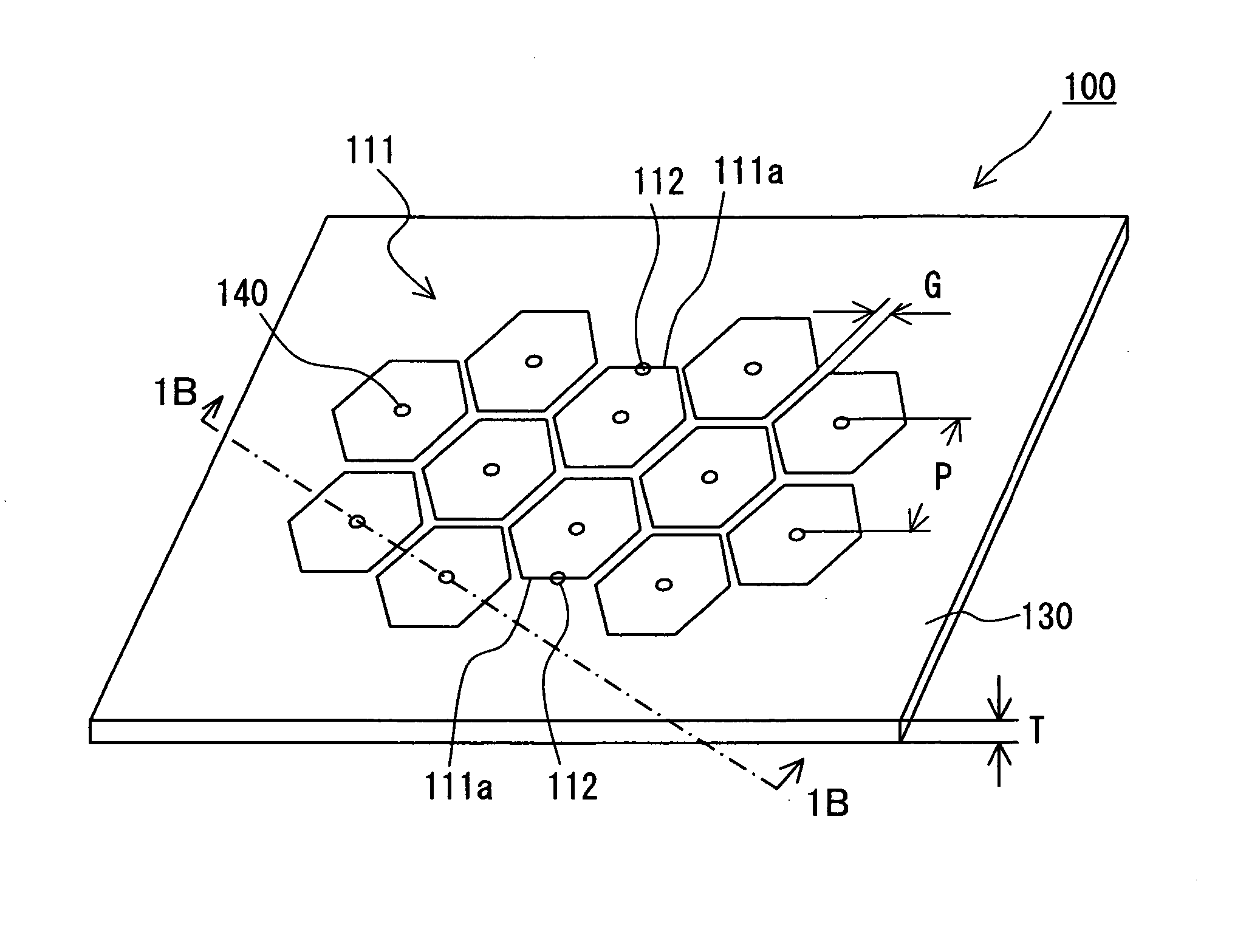
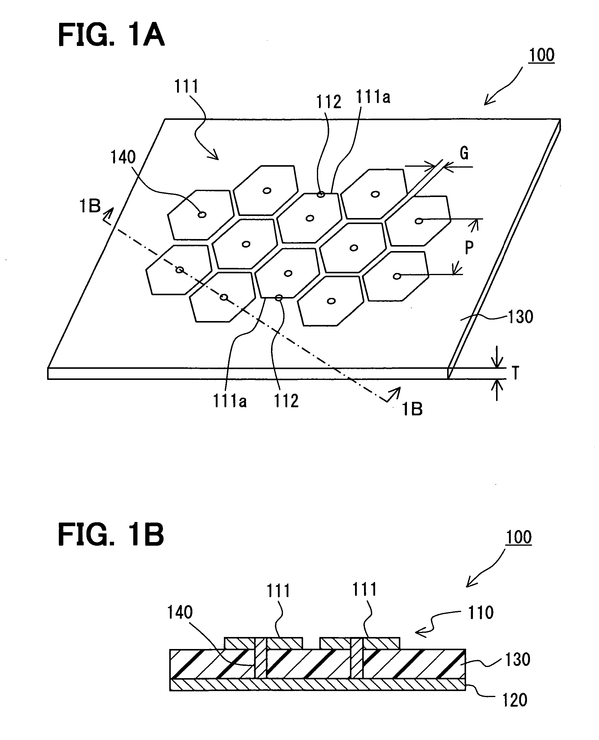
[0032] As shown in FIGS. 1A and 1B, an antenna 100 comprises plural elements 111 constituting a first conductive layer 110, a second conductive layer 120 disposed at a predetermined thickness T from the first conductive layer, a dielectric substrate 130 provided between the first conductive layer 110 and the second conductive layer 120, and conductive connecting members 140 for respectively electrically connecting the elements 111 and the second conductive layer 120.

[0033] The first conductive layer 110 has plural elements 111 made of conductive materials. The elements 111 are disposed adjacently to and separated from each other on a same plane of the dielectric substrate 130. The shape and size of the plural elements 111 are not limited as long as capacitors can be formed between adjacent elements 111. However, if all of the elements are substantially identical in shape and size, it becomes easy to design them. Efficient disposition of the elements 111 contributes to miniaturizati...

second embodiment

[0064] In this embodiment, the shape of the elements 111 in a plane direction is a square. In the case of a square, like the case of a regular hexagon, the elements 111 can be efficiently disposed. Moreover, manufacturing costs can be reduced because of easier manufacturing than the cases of other polygonal shapes.

[0065] As shown in FIG. 10A, in a construction in which the elements 111 are disposed so that the sides of the elements 111a each having the power feeding section 112 are opposed to each other, when the power feeding sections 112 are provided in the center of opposing sides, or in the center of opposite sides of opposing sides, the reflection coefficients of the power feeding sections 112 can be reduced. That is, preferably, the antenna 100 can be efficiently operated. As shown in FIG. 10B, in a construction in which the elements 111 are disposed so that vertexes of the elements 111a each having the power feeding section 112 are opposed to each other, when the power feedi...

third embodiment

[0067] In this embodiment, to connect to the outside, a microstrip line 150 is provided on a surface of the dielectric substrate 130 on which elements are formed, so that power is fed to the antenna 100 via the microstrip line 150. Specifically, in the antenna 100 in the first or second embodiment, the power feeding sections 112 are provided in the centers of opposite sides of opposing sides (or opposing vertexes) of two elements 111a, and the elements are disposed so that the sides or vertexes in which the power feeding sections 112 do not approach other elements 111. The microstrip lines 150 are respectively connected to the locations of the power feeding sections 112 and connected to the outside of the antenna 100 (dielectric substrate 130). Power is fed to the microstrip lines 150 so that phases of radio frequency signals are opposite to each other. That is, if the phase of one radio frequency signal is 0 degree, the phase of the other is 180 degrees. Such microstrip line 150 ca...


PUM


Abstract

An antenna comprises a first conductive layer, a second conductive layer and an LC resonance circuit. The first conductive layer has plural elements and is disposed adjacently to each other. The second conductive layer is disposed at a predetermined distance from the first conductive layer via a dielectric substrate. The LC resonance circuit comprises connection for electrically connecting the elements and the second conductive layer. The LC resonance circuit takes a resonance state in which impedance becomes high in the operating frequency of the antenna. Of the plural elements, a power feeding section is provided in each of any two adjacent elements. Power is fed to the power feeding sections during transmission so that signals of the operating frequency are opposite in phase, and signals of the operating frequency inputted to the antenna are outputted in opposite phase from the power feeding sections during reception.

Description

CROSS REFERENCE TO RELATED APPLICATION [0001] This application is based on and incorporates herein by reference Japanese Patent Application No. 2005-290312 filed on Oct. 3, 2005. FIELD OF THE INVENTION [0002] The present invention relates to an antenna and radio device using it, and more particularly to a flat antenna formed on a dielectric substrate. The present invention also relates to methods of designing and measuring operating frequency of an antenna. BACKGROUND OF THE INVENTION [0003] A patch antenna has a typical structure of a flat antenna. The patch antenna uses a rectangular or circular metallic pattern formed on a surface of a dielectric substrate as a radiator, the metallic pattern resonating in radio frequency signals sent or received. The patch antenna uses a metallic film formed on a back surface of the substrate as a ground electrode. Since general patch antennas have a ground electrode on the back surface, they exhibit the directivity that radio waves are directed ...

Claims


Application Information

Patent Timeline
Patent Type & Authority Applications(United States)
IPC IPC(8): H01Q1/38H01Q15/24
CPCH01Q9/0421H01Q9/065H01Q21/065H01Q15/0053H01Q15/008H01Q3/22H01Q1/38H01Q23/00
Inventor MATSUGATANI, KAZUOKITANAKA, MAKOTOKIM, DOWONKIM, MOONIL
Owner DENSO CORP
Why Eureka
Try Eureka