
Liquid crystal display and method of manufacturing the same

a technology of liquid crystal display and liquid crystal, which is applied in the direction of instruments, non-linear optics, optics, etc., can solve the problems of narrow viewing angle and reduce operation characteristics such as brightness and light transmittance, and achieve the effect of easy removal control

Inactive Publication Date: 2007-04-05
SAMSUNG ELECTRONICS CO LTD
View PDF4 Cites 12 Cited by
  • Summary
  • Abstract
  • Description
  • Claims
  • Application Information

AI Technical Summary

Benefits of technology

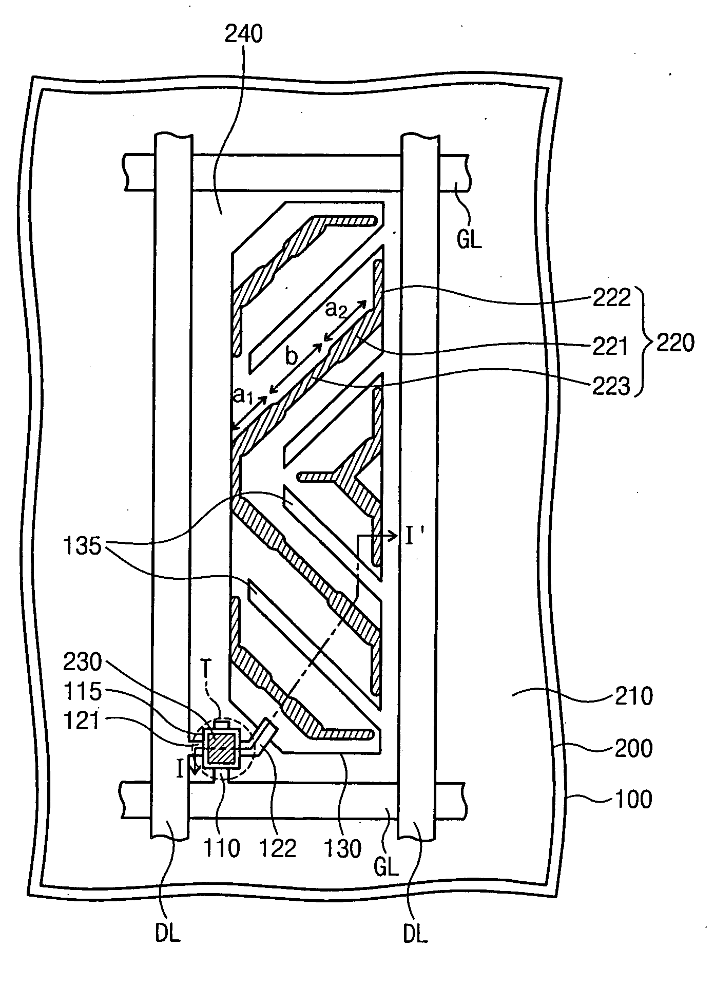
[0012] The cutouts and the protrusion are spaced apart from each other and interact to allow formation of multiple regions or domains. In another embodiment, a spacer formed of the same material as and higher than the protrusion is interposed between the first substrate and the second substrate. The spacer and the protrusion may be formed at the same time by patterning the same photoresist film. Because the spacer is formed at a height greater than the protrusion, the photoresist film is formed with a greater thickness than the height of the protrusion. This enables easier control of the removal of the photoresist film for forming protrusions of different sizes. The protrusion includes a first portion inclined against the gate line or the data line and a second portion parallel to the gate line or the data line having a smaller size than the first portion.

Problems solved by technology

One disadvantage of a conventional LCD is that it has a narrow viewing angle.
However, boundary conditions at the edge of a pixel prevents the molecules of the LC at the pixel edge from being tilted as desired, thereby reducing operation characteristics such as brightness and light transmittance.

Method used


Image

  • Liquid crystal display and method of manufacturing the same
  • Liquid crystal display and method of manufacturing the same
  • Liquid crystal display and method of manufacturing the same

Examples


Embodiment Construction

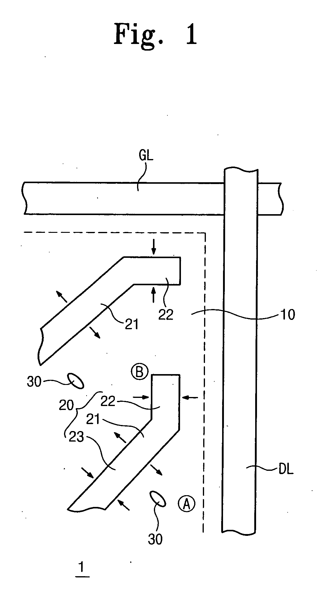
[0023]FIG. 1 is a schematic plan view of a substrate of an LCD device according to an embodiment of the present invention. A substrate 1 includes a transparent electrode 10, a protrusion 20 protruding upward, and a liquid crystal (LC) 30 disposed over substrate 1. One or more protrusions 20 are formed on transparent electrode 10, and the molecules of LC 30 are aligned at a tilt angle by applying voltage. The LCD device includes an upper and a lower substrate. Substrate 1 can be either. If substrate 10 is a lower substrate, transparent electrode 10 is a pixel electrode and the lower substrate includes a gate line GL and a crossing data line DL defining a pixel (dotted line). If substrate 10 is an upper substrate, transparent electrode 10 is a common electrode forming on the whole substrate with no separation between pixel regions.

[0024] Generally, protrusion 20 is formed on the upper substrate by patterning a photoresist, as will be described in detail below, because of manufacturin...


PUM


Abstract

A liquid crystal display device includes a substrate, liquid crystal disposed on the substrate, and a protrusion to influence on the alignment of the molecules of the liquid crystal to increase a viewing angle. The protrusion includes portions with different sizes, depending on the desired control power of the protrusion on the alignment of the molecules. That is, the portion size increases in the area where more control power is desired, and the portion size decreases in the area where less control power is desired. The protrusion is formed by depositing and pattering a thick photoresist. At the same time, a spacer can be formed.

Description

CROSS-REFERENCE TO RELATED APPLICATION [0001] This application claims priority to Korean Patent Application No. 2005-0093565 filed on Oct. 5, 2005, the disclosure of which is hereby incorporated herein by reference in its entirety for all purposes. BACKGROUND [0002] 1. Field of the Invention [0003] The present invention relates generally to liquid crystal displays (LCDs) and methods of manufacturing the same. [0004] 2. Description of Related Art [0005] A liquid crystal display (LCD) is widely used in flat panel displays. An LCD includes two panels or substrates with field-generating electrodes (i.e., a pixel electrode and a common electrode) and a liquid crystal (LC) layer interposed therebetween. The LCD displays images by applying voltages to the electrodes to generate an electric field in the LC layer, which determines orientations of LC molecules in the LC layer to adjust polarization of incident light and brightness of the LCD. [0006] The LC has a dielectric anisotropy and a re...

Claims


Application Information

Patent Timeline
IPC IPC(8): G02F1/1343
CPCG02F1/133707G02F1/13394G02F1/134336G02F2001/136231G02F2201/123G02F2201/40G02F1/136231G02F1/1337G02F1/1343
Inventor JUNG, MIN-SIKJANG, YUN
Owner SAMSUNG ELECTRONICS CO LTD
Learn More