Semiconductor device, method for assembling semiconductor device

Active Publication Date: 2007-04-12
SONY COMPUTER ENTERTAINMENT INC
View PDF3 Cites 11 Cited by
  • Summary
  • Abstract
  • Description
  • Claims
  • Application Information

AI Technical Summary

Benefits of technology

[0011] The semiconductor chip may be put on the package substrate with its circuit side facing the package substrate, wherein heat is dissipated from its upper side opposite to the circuit side. The sealing resin may seal around the periphery of the semiconductor chip so that the upper side of the semiconductor chip is exposed to the atmosphere. According to this aspect, the heat radiator makes contact with a flip-chip implemented semiconductor chip. Therefore, heat may be directly radiated from the upper side of the semiconductor chip, thereby improving heat radiation efficiency.
[0012] Part of the fixing member may be buried in the sealing resin so that a hook formed on the

Problems solved by technology

However, this method increases the number of components and tasks for assembling the semiconductor device.
Furthermore, increasing the

Method used


Image

  • Semiconductor device, method for assembling semiconductor device
  • Semiconductor device, method for assembling semiconductor device
  • Semiconductor device, method for assembling semiconductor device

Examples


Embodiment Construction

[0034] The invention will now be described by reference to the preferred embodiments. This does not intend to limit the scope of the present invention, but to exemplify the invention.

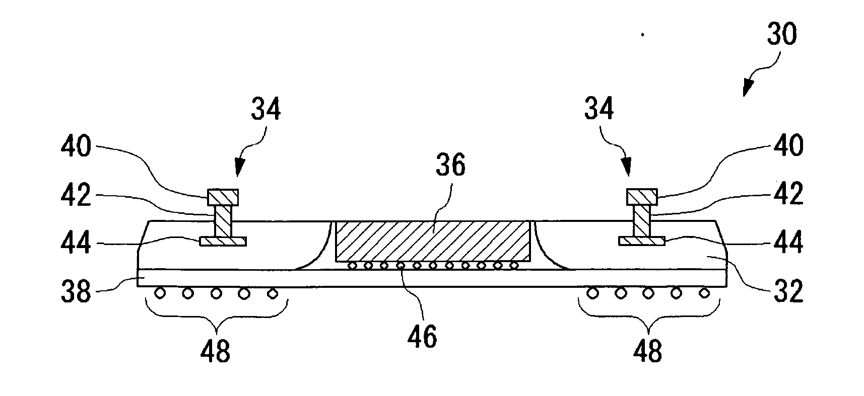
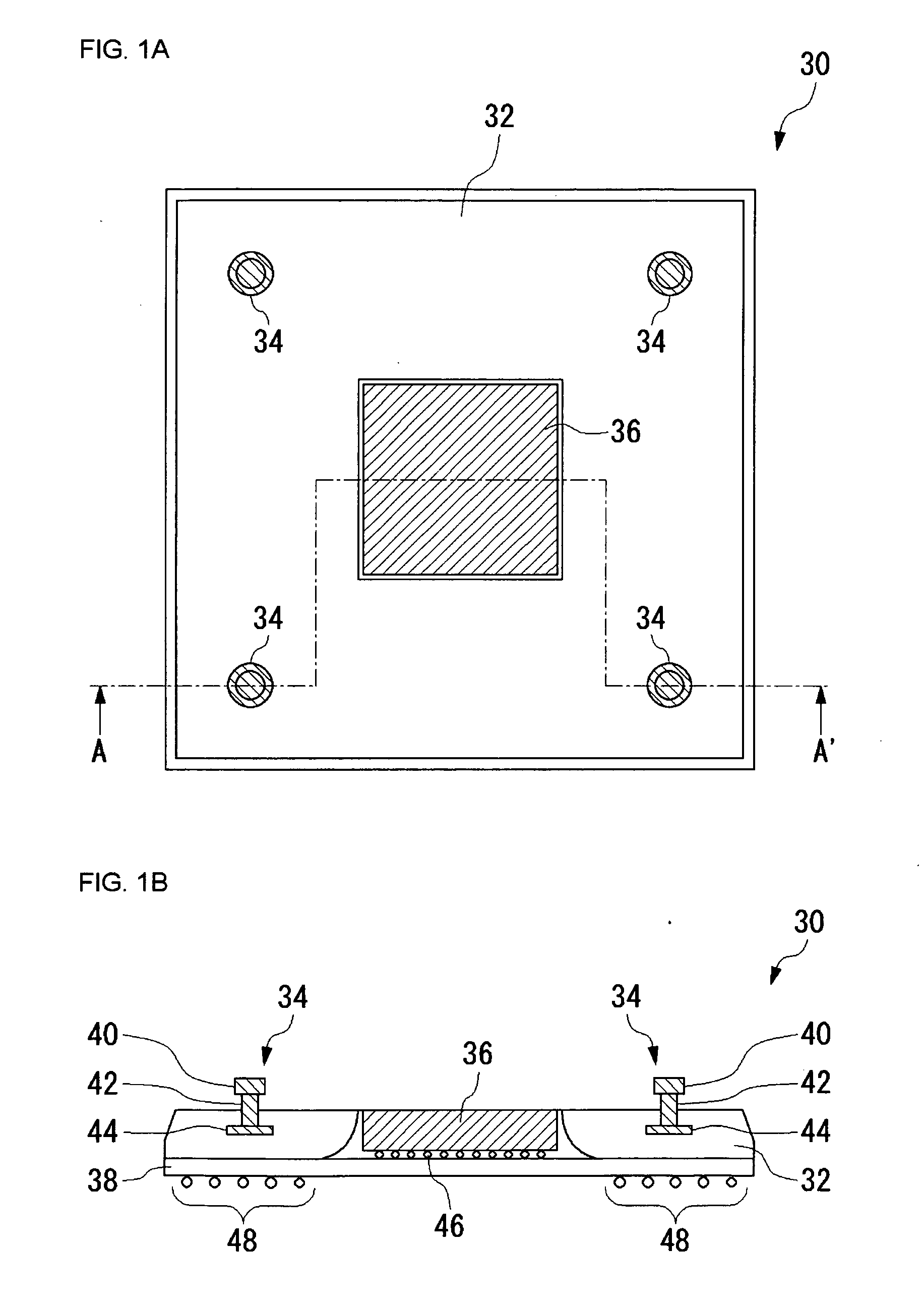
[0035]FIG. 1A is a plane view of a package substrate 30 according to one embodiment of the invention. FIG. 1B is a cross-sectional view along line A-A′ of the package substrate in FIG. 1A. The package substrate 30 comprises a board 38, a semiconductor chip 36 flip-chip implemented on the board 38, and a sealing resin 32 sealing around the periphery of the semiconductor chip 36.

[0036] The board 38 has multilayered wiring structure that insulating films and wiring layers are laminated alternately. On each of ball land areas (not shown) formed on the back side of the board 38, a BGA ball 48 is placed respectively. The package substrate 30 serves as an intermediate plate to mount the semiconductor chip 36 on an implementation substrate. On the side where the semiconductor chip 36 is equipped on the board ...


PUM


Abstract

A semiconductor chip 36 is mounted on a package substrate 30 with its circuit side facing to a board 38. Heat is dissipated from an upper side of the semiconductor chip 36 opposite to the circuit side. A sealing resin 32 seals around the periphery of the semiconductor chip 36 so that the upper side of the semiconductor chip 36 is exposed to atmosphere. A fixing member 34 is buried in the sealing resin 32 so that a hook 40 formed on the tip of the fixing member 34 extends above the upper side of the semiconductor chip 36. A spreader 10 dissipates heat emitted from the semiconductor chip 36. A guiding slot 12 is formed on the side facing to the package substrate 30 of the spreader 10. The hooks 40 of the fixing members 34 are inserted into the guiding slots 12 respectively, and then the spreader 10 is rotated by predetermined angle against the package substrate 30. Then, the hooks 40 travel along the slots 12. Through such process, the spreader 10 is pulled to come into contact with the upper side of the semiconductor chip 36.

Description

BACKGROUND OF THE INVENTION [0001] 1. Field of the Invention [0002] The present invention relates to technology for attaching a heat radiator or the like to a package substrate. [0003] 2. Description of the Related Art [0004] Various types of semiconductor chips, such as a CPU (Central Processing Unit) and a DSP (Digital Signal Processor), which controls electronic equipments, are constructed of various electronic components including active elements, such as transistors and passive elements, such as capacitors. Part of electric energy for driving these electronic components is converted into thermal energy and dissipated as heat. The performance of the electronic components typically has temperature dependence. Then, the dissipated heat has an inverse effect on the performance of the electronic components, and by extension that of the semiconductor chips. Thus, technologies for cooling the semiconductor chips are of significant importance in controlling the electronic devices prope...

Claims


Application Information

Patent Timeline
IPC IPC(8): H01L23/48
CPCH01L23/40H01L23/4006H01L2023/405H01L2023/4062H01L2023/4087H01L2224/16H01L2224/73253H01L2924/01078H01L2924/01079H01L2924/15311
Inventor YAZAWA, KAZUAKI
Owner SONY COMPUTER ENTERTAINMENT INC
Why Eureka
Try Eureka