Thin film transistors, liquid crystal display device and electronic apparatus using the same

a technology of thin film transistors and liquid crystal displays, applied in semiconductor devices, semiconductor/solid-state device details, instruments, etc., can solve the problem of inability to increase the number of production steps, and achieve the effect of enhancing heat radiation efficiency, increasing the number of production steps, and not deteriorating characteristics

Inactive Publication Date: 2005-08-23
BOE TECH GRP CO LTD
View PDF26 Cites 11 Cited by
  • Summary
  • Abstract
  • Description
  • Claims
  • Application Information

AI Technical Summary

Benefits of technology

[0006]In view of the foregoing problems, an object of the present invention is to provide: a TFT circuit having a structure for enhancing the heat radiation efficiency without increasing the number of production steps, in which its characteristics do not deteriorate and its reliability does not decline; and a liquid crystal display device provided with an active matrix substrate using the TFT circuit as a driving circuit.
[0007]In other words, not by adding a new layer to TFTs, but by enlarging part of each component of the TFTs, the heat-radiating efficiency from the TFTs is enhanced.

Problems solved by technology

Accordingly, even when the heat-radiating extension is provided, the number of production steps cannot be increased.

Method used


Image

  • Thin film transistors, liquid crystal display device and electronic apparatus using the same
  • Thin film transistors, liquid crystal display device and electronic apparatus using the same
  • Thin film transistors, liquid crystal display device and electronic apparatus using the same

Examples


embodiment 1

[Embodiment 1]

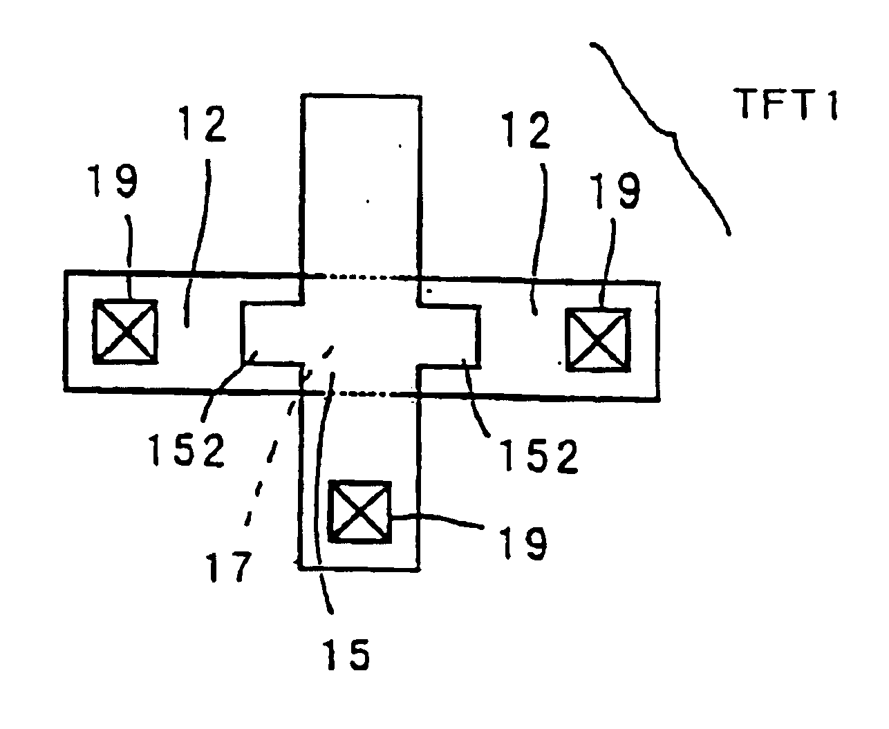
[0040]FIG. 1 is an explanatory expanded view showing the plane structure of a TFT used for a TFT circuit according to Embodiment 1. In TFT 1 shown in this figure, among gate electrode 15, channel region 17 opposed thereto with a gate insulating film (not shown) provided therebetween, and source-drain region 12 connected to the channel region 17, the gate electrode 15 is provided with extensions 151 (radiating extensions) extending from its ends at both sides along the channel longitudinal direction. 19 denotes contact holes used so that wiring layers (not shown) such as a source-drain wiring layer and a gate wiring layer can be electrically connected to the source-drain region 12 and the gate electrode 15.

[0041]In the TFT 1 having the above structure, the extensions 151 are provided on the gate electrode 15, which is composed of a metal film (aluminum layer / conductive film) having a higher thermal conductivity than that of a silicon oxide film or silicon film. Thus, in...

embodiment 2

[Embodiment 2]

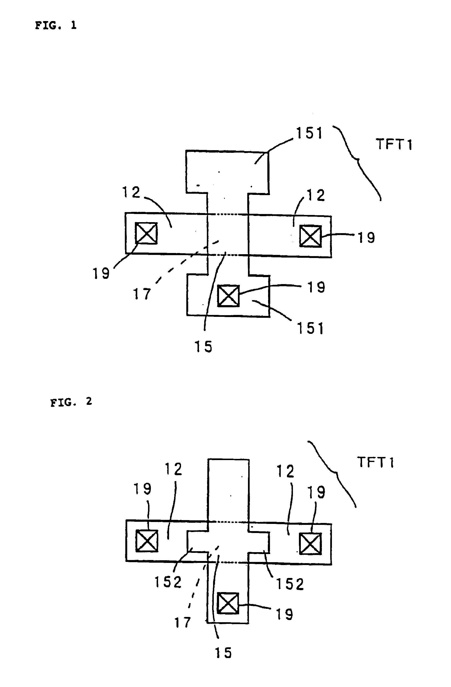
[0042]FIG. 2 is an explanatory expanded view showing the plane structure of a TFT used for a TFT circuit according to Embodiment 2. In the TFT 1 shown in this figure, among gate electrode 15, channel region 17, and source-drain region 12, the gate electrode 15 is provided with extensions 152 (heat-radiating extensions) extending from its central portion at both sides along the channel longitudinal direction. Here, the extensions 152B are narrower than the channel width and are positioned almost in the center of the width of the channel region 17. 19 denotes contact holes used so that wiring layers (not shown) such as a source-drain wiring layer and a gate wiring layer can be electrically connected to the source-drain region 12 and the gate electrode 15.

[0043]Even in the TFT 1 having the above structure, similarly to Embodiment 1, the extensions 152 are provided on the gate electrode 15, which is composed of a metal film (aluminum layer / conductive film) having a higher ...

embodiment 3

[Embodiment 3]

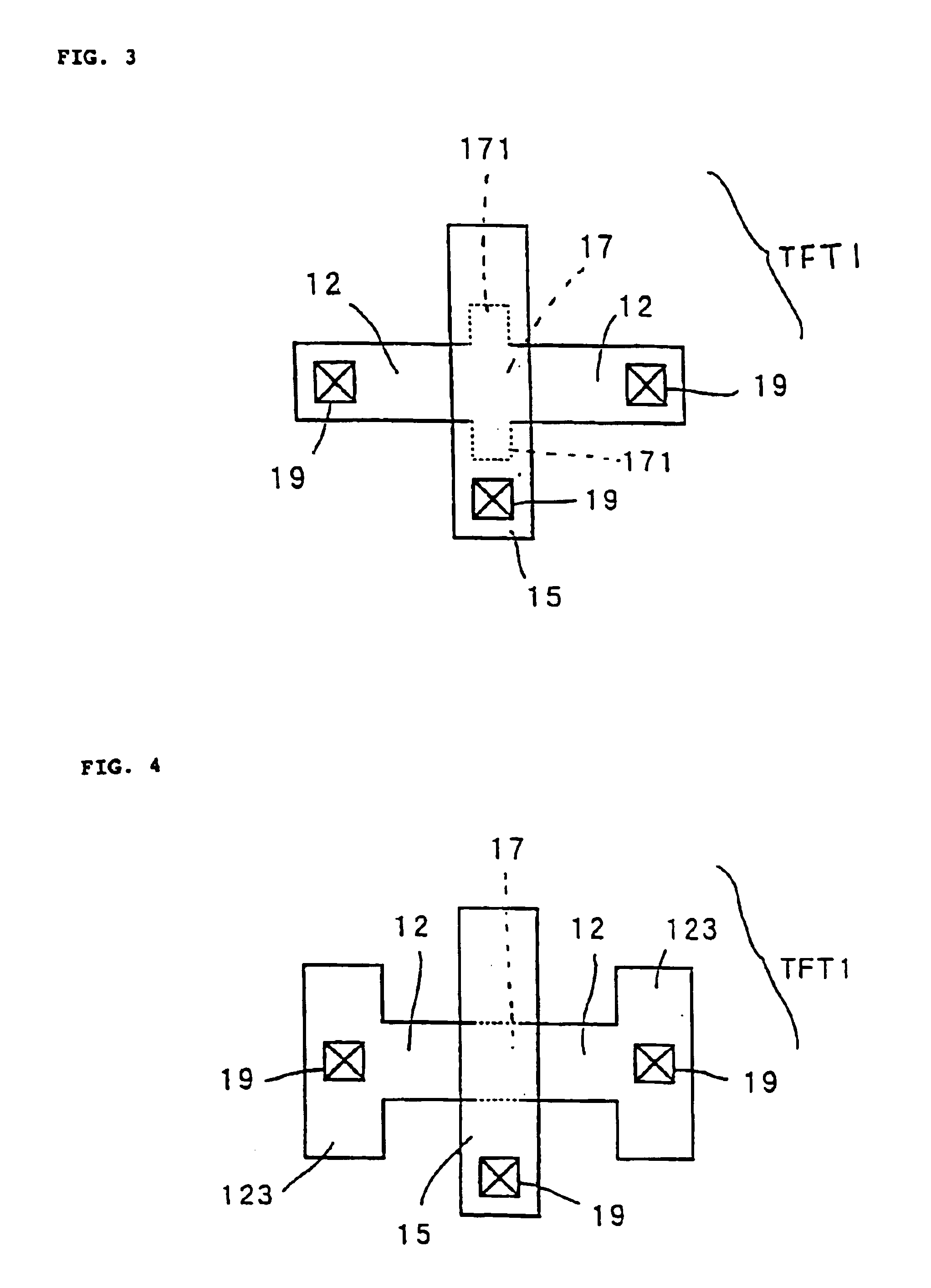
[0046]FIG. 3 is an explanatory expanded view showing the plane structure of a TFT used for a TFT circuit according to Embodiment 3. In the TFT 1 shown in this figure, among gate electrode 15, channel region 17, and source-drain region 12, the channel region 17 is provided with extensions 171 (heat-radiating extensions) extending from its central portion at both sides along the extending direction (channel width direction) of the gate electrode 15. Here, the extensions 171 are narrower than the width of the gate electrode 17 and are positioned almost in the center of the width of the gate electrode 15. 19 denotes contact holes used so that wiring layers (not shown) such as a source-drain wiring layer and a gate wiring layer can be electrically connected to the source-drain region 12 and the gate electrode 15.

[0047]In the TFT 1 having the above structure, the extensions 171 are provided on the channel region 17, which is composed of a silicon film (semiconductor film) ha...


PUM

PropertyMeasurementUnit
thicknessaaaaaaaaaa
thicknessaaaaaaaaaa
thicknessaaaaaaaaaa

Abstract

In a TFT including on the surface side of a substrate a channel region opposed to a gate electrode, with a gate insulating film provided therebetween, and a source-drain region connected to the channel region, and a TFT including a source-drain wiring layer electrically connected to the source-drain region, and a gate wiring layer electrically connected to the gate electrode, at least one component part composed of a conductive film or a semiconductor film, among the component parts of each TFT, is provided with a heat-radiating extension extended from the component part itself for enhancing the heat-radiating efficiency from the component part.

Description

[0001]This is a Division of Application No. 09 / 077,207 filed May 26, 1998, now U.S. Pat. No. 6,770,930, which is a National Stage Application of PCT / JP97 / 03626, filed Oct. 8, 1997 in Japan, which claims priority of Japanese Application No. 8-268288, filed Oct. 9, 1996 in Japan The entire disclosure of the prior applications is hereby incorporated by reference herein in its entirety.DESCRIPTION OF RELATED ART[0002]TFTs and a TFT circuit widely used as an active matrix substrate for a liquid crystal display device are formed so that, as shown in FIG. 14 and FIG. 15, gate electrode 15Q, source-drain region 12Q and channel region 17Q each have an almost rectangular plane shape without extending in its side direction. In addition, in each TFT 1Q in FIG. 15, silicon films forming source-drain region 12Q and channel region 17Q are patterned in an independent insular shape. Here, when various types of TFT circuits are formed from TFTs, a wiring layer 801Q formed to have a uniform width is u...

Claims


Application Information

Patent Timeline
Patent Type & Authority Patents(United States)
IPC IPC(8): H01L23/34H01L21/70H01L29/417H01L29/423H01L23/367H01L27/12H01L21/84H01L29/40G02F1/13G02F1/1362G02F1/136G02F1/1368H01L21/77H01L29/786
CPCH01L23/3672H01L29/41725H01L29/41733H01L29/42384H01L29/78696H01L27/124G02F1/13454H01L2924/0002H01L2924/00H01L29/786
Inventor INOUE, SATOSHIYUDASAKA, ICHIO
Owner BOE TECH GRP CO LTD
Why Eureka
Try Eureka