Wafer singulation process

a technology of wafers and wafers, applied in the direction of semiconductor/solid-state device manufacturing, basic electric elements, electric instruments, etc., can solve the problems of time-consuming and costly process, singulation process can damage parts of dies, including the sides of dies,

Inactive Publication Date: 2007-04-19
INFINEON TECH AMERICAS CORP
View PDF34 Cites 84 Cited by
  • Summary
  • Abstract
  • Description
  • Claims
  • Application Information

AI Technical Summary

Problems solved by technology

Singulating the dies of the wafer, for example, by sawing the wafer along the streets after the wafer is complete, including metal layers on the back or

Method used


Image

  • Wafer singulation process
  • Wafer singulation process
  • Wafer singulation process

Examples


Embodiment Construction

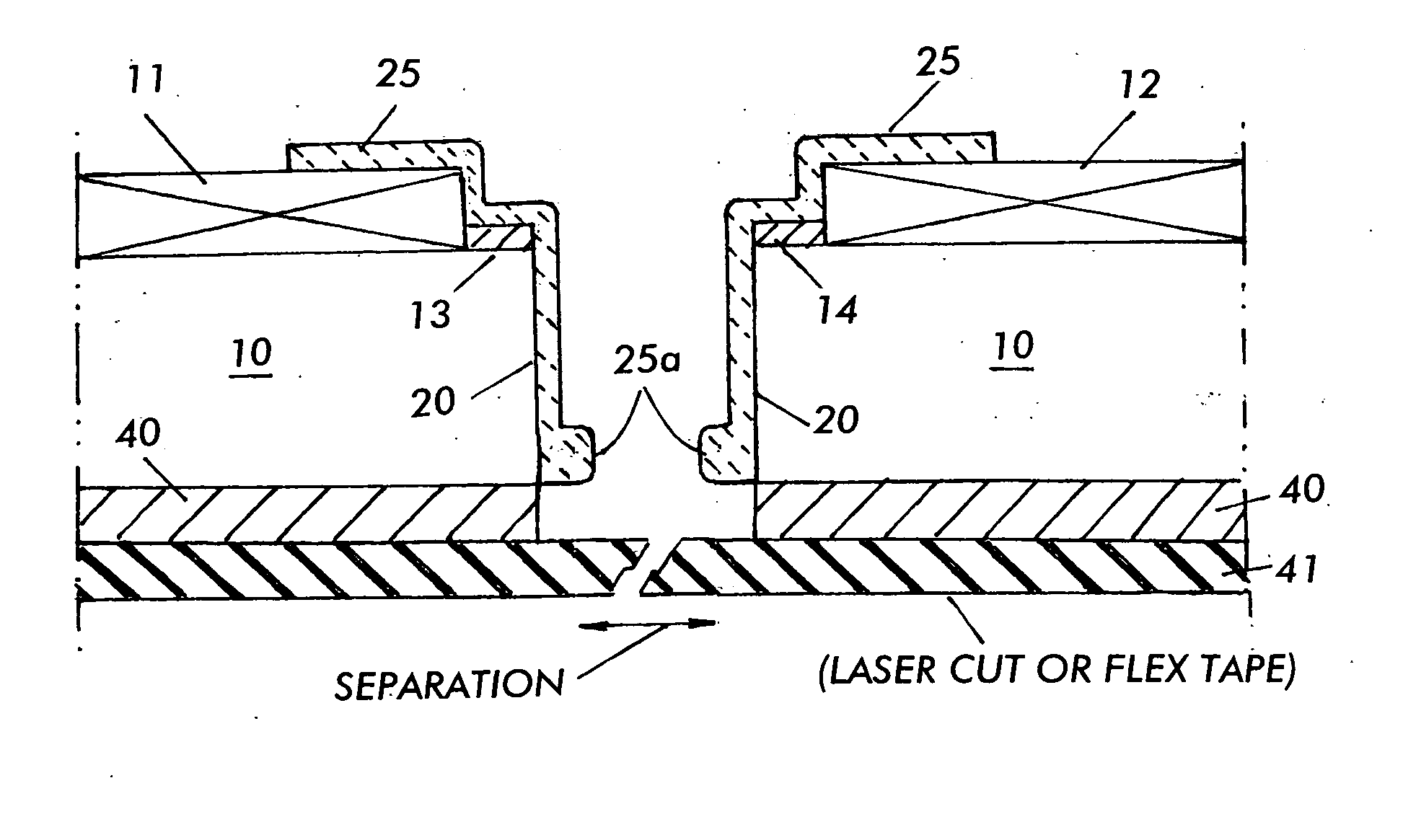
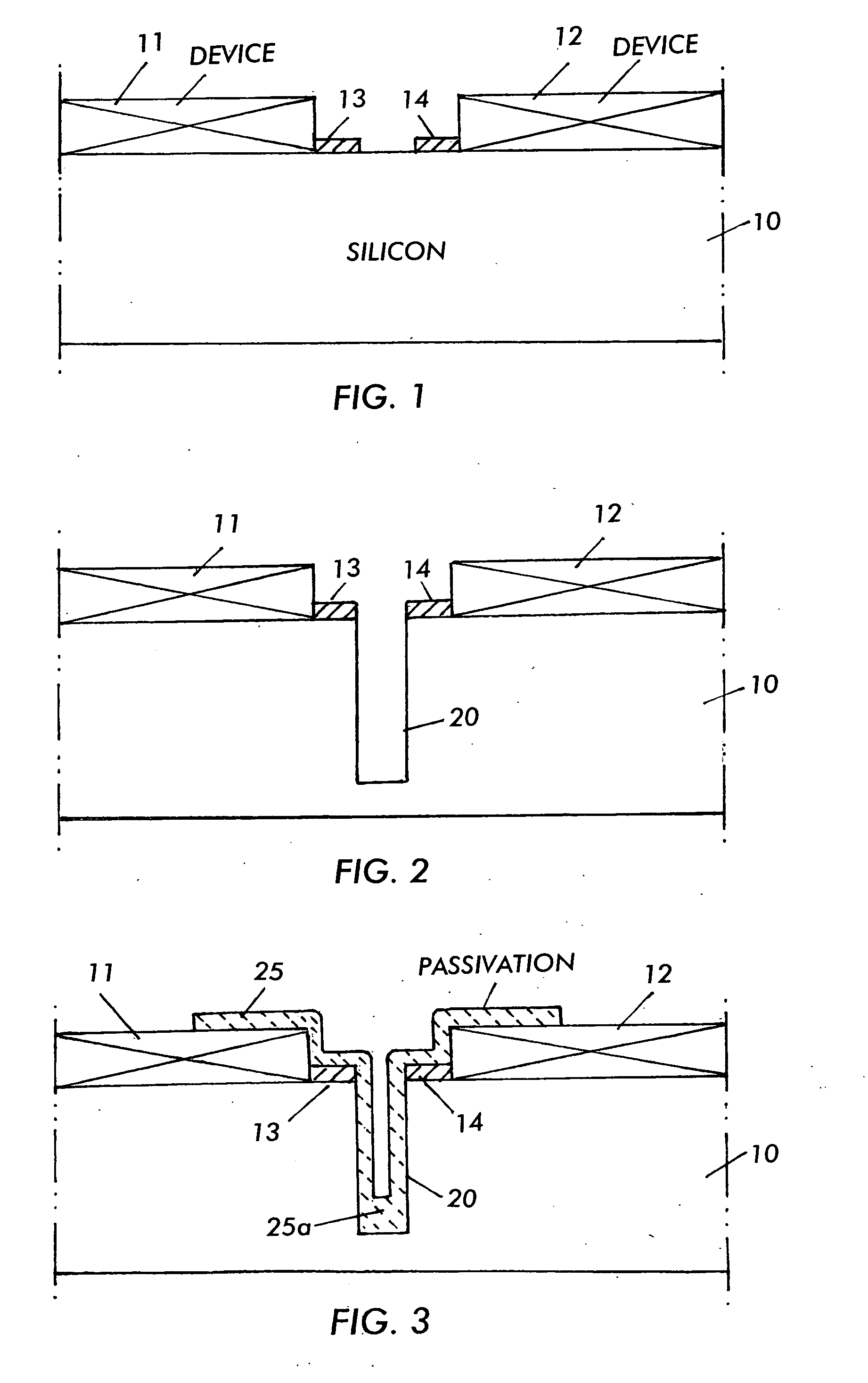
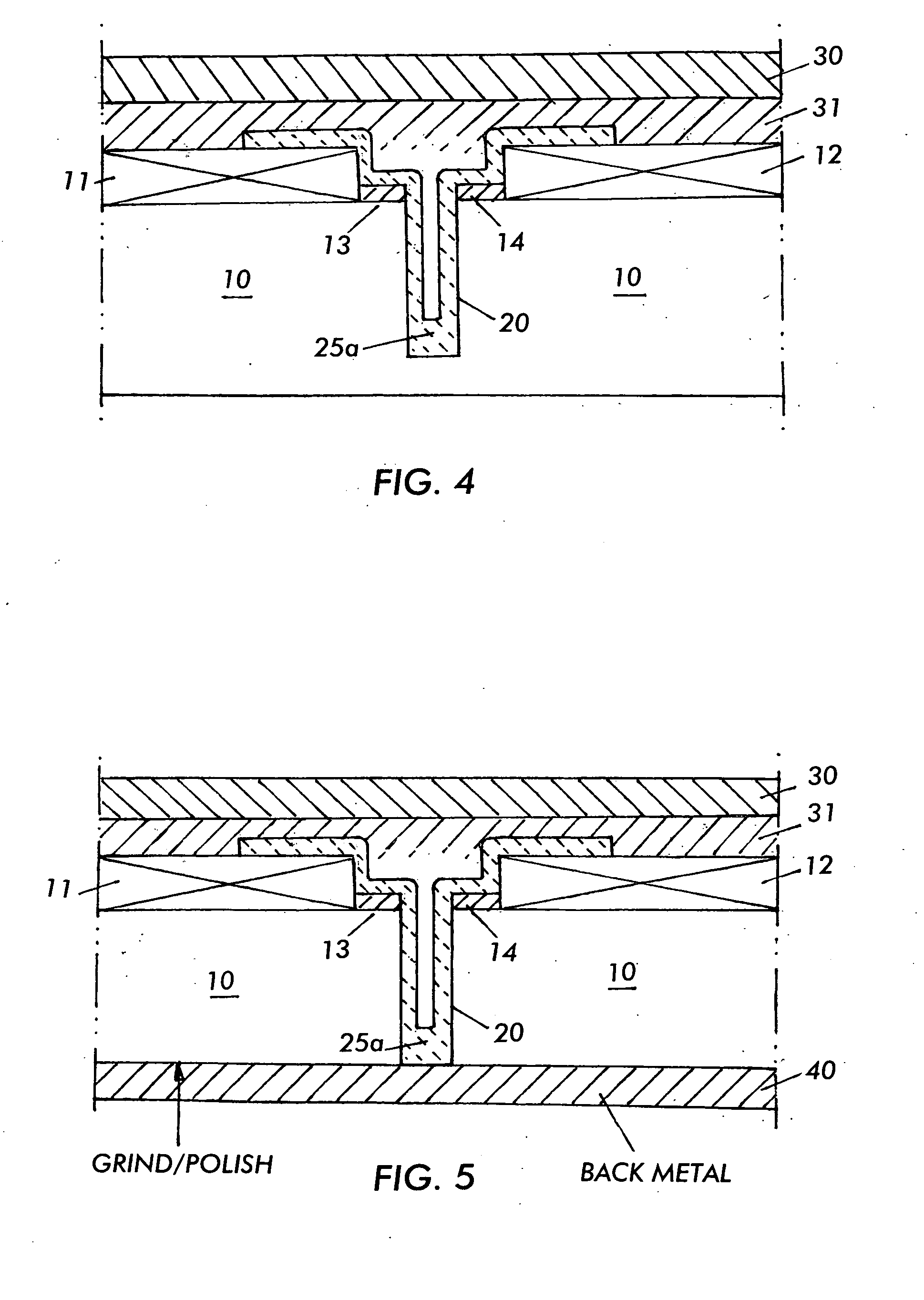
[0015] A method of singulating the dies of the wafer will now be described with reference to FIGS. 1-6. A silicon wafer 10 has several laterally spaced devices, such as devices 11 and 12 of any desired device type and form necessary for the dies which they comprise. The wafer 10 can be of any desired material, such as silicon, GaN, SiC and the like. Any number of separate devices 11 and 12 can be provided as part of the wafer 10, such as identical vertical conduction MOSFETs with a planar or a trench topology.

[0016] A mask layer is then deposited along the first side of the wafer and a portion of the mask is removed to leave mask deposits 13 and 14, thus exposing the top of the wafer 10 as an etch window so that a trench 20 may be etched. FIG. 2 shows trench mask portions 13 and 14 between devices 11 and 12. Alternatively, the trench may be cut instead of etched. Cutting could be easily performed since a street could be cut along the entire length of the wafer 10 to the desired dep...


PUM


Abstract

A method of singulating a semiconductor die from a wafer is provided. The method includes etching or cutting several trenches into the wafer from a front surface of the wafer, such that each trench extends along an entire side of the die; depositing a passivation layer into the trenches to form a passivation plug on at least a bottom of the trenches to protect the dies and immobilize them during singulation; and forming a rigid carrier layer or plate at the first side of the wafer to secure the dies. The wafer is then ground from the back side to expose the bottom of each trench, a metal layer is formed on the back surface of the wafer; dicing tape is added, the carrier layer is removed, and the die is separated from the wafer by laser cutting or by flexing the tape.

Description

RELATED APPLICATION [0001] The present application claims priority from U.S. Provisional Application No. 60 / 727,711, filed Oct. 18, 2005, which is incorporated in full herein by reference.FIELD OF THE INVENTION [0002] This invention relates to semiconductor device processing and more specifically relates to a novel process for singulating semiconductor dies from a wafer. BACKGROUND OF THE INVENTION [0003] Semiconductor dies such as diodes, transistors and the like are commonly processed (formed) simultaneously in a large area wafer. Such wafers may be made of monocrystaline silicon or other materials, such as gallium nitride on a suitable substrate such as silicon or the like. After the processing steps are completed, the wafers are singulated, separating the die from the wafer. This “dicing,” separation or singulating operation is commonly carried out by sawing through the “streets” between the dies within the wafers. [0004] Singulating the dies of the wafer, for example, by sawing...

Claims


Application Information

Patent Timeline
IPC IPC(8): H01L21/76
CPCH01L21/78
Inventor MONTGOMERY, ROBERT
Owner INFINEON TECH AMERICAS CORP
Why Eureka
Try Eureka