Board placement method and system for defective printed circuit board panel having multiple interconnected printed circuit board units

a technology of printed circuit board and interconnected units, which is applied in the direction of circuit inspection/indentification, manufacturing tools, coupling device connections, etc., can solve the problems of waste of resources, high repair rate, and high defect rate of printed circuit board panels having multiple interconnected pcb units during manufacture, so as to achieve the effect of enhancing the precision and stability of board placement and board repair and increasing the repair ra

Inactive Publication Date: 2007-04-19
KU SHING SAN
View PDF5 Cites 16 Cited by
  • Summary
  • Abstract
  • Description
  • Claims
  • Application Information

AI Technical Summary

Benefits of technology

[0011] Therefore, an object of the present invention is to provide a board placement method and system for a printed circuit board panel having multiple interconnected PCB units, which can enhance repair precision and stability.
[0013] Still another object of the present invention is to provide a board placement method and system for a printed circuit board panel having multiple interconnected PCB units, which can enhance repair rate through automated operations, and which permits fast mass production.
[0019] In step (A), the micro-adjusting unit includes a micro-adjusting table disposed below the support seat and capable of enabling the support seat to move relative to the work surface along an X-axis direction, a Y-axis direction, and a Z-axis direction. A first axial line passing through midpoints of two opposite sides of the support seat, a second axial line passing through midpoints of two other sides of the support seat, and a third axial line at the intersection of the first and second axial lines and parallel to the Z-axis direction are defined. The micro-adjusting table can drive the support seat to rotate relative to the work surface with the first, second and third axial lines as axes, respectively.
[0022] In step (C), the micro-adjusting table drives the support seat to move horizontally along the X-axis direction and the Y-axis direction, and drives the support seat to rotate, with the third axial line as axis, so as to micro-adjust the good PCB unit to the target position.
[0023] In step (E), a work path of a laser of the measuring unit is predetermined in the computer device. In step (B), the laser is employed to measure respective height differences between connecting portions of the good PCB unit and corresponding positions of the printed circuit board panel and, in step (C), the micro-adjusting table is driven to move along the Z-axis direction, and to rotate the support seat, with the first and second axial line as axes, so as to achieve a state of levelness between the connecting portions of the good PCB unit and the corresponding positions of the printed circuit board panel.
[0030] In the board placement method and system for a printed circuit board panel having multiple interconnected PCB units of the present invention, through the use of a computer device to control measurement, glue injection, glue clearing, and curing, as well as automated operation of the micro-adjusting unit, precision and stability of board placement and board repair can be considerably enhanced, and the repair rate can be increased to be suitable for fast mass production.

Problems solved by technology

The defective product rate for printed circuit board panels having multiple interconnected PCB units during manufacture is about 5% to 7%.
Since component insertion for a printed circuit board panel having multiple interconnected PCB units on a production line is generally set with fixed path values, whenever there is a defective PCB unit in the printed circuit board panel, most manufacturers will simply dispose of the same as non-usable, thereby resulting in waste of resources.
However, such a process is time-consuming and inefficient, and is not economically effective.
However, the aforesaid patent failed to disclose an automated process for performing moving alignment, which may be difficult in practice.
Therefore, even if the good PCB unit is positioned according to the process disclosed in the aforesaid patent, if there is a drop between the good PCB unit and the printed circuit board panel at the joint, the printed circuit board panel will still be determined to be a defective printed circuit board panel.
However, performing manual visual inspection concurrently with alignment and positioning is likely to affect precision.
Besides, since the quality of the operators is inconsistent, unstable quality problems, such as a high redo rate, a low repair rate, etc., may result.
In addition, the process of board replacement is complicated, and the speed of manual operation is slow, thereby resulting in low production capacity and rendering fast mass production impossible.

Method used


Image

  • Board placement method and system for defective printed circuit board panel having multiple interconnected printed circuit board units
  • Board placement method and system for defective printed circuit board panel having multiple interconnected printed circuit board units
  • Board placement method and system for defective printed circuit board panel having multiple interconnected printed circuit board units

Examples


Embodiment Construction

[0047] Before the present invention is described in greater detail, it should be noted that like elements are denoted by the same reference numerals throughout the disclosure.

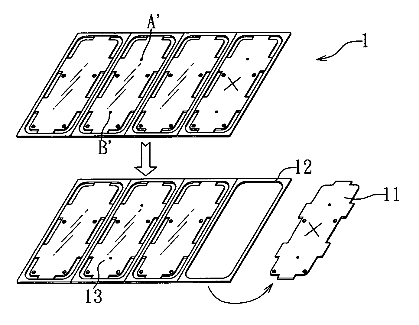
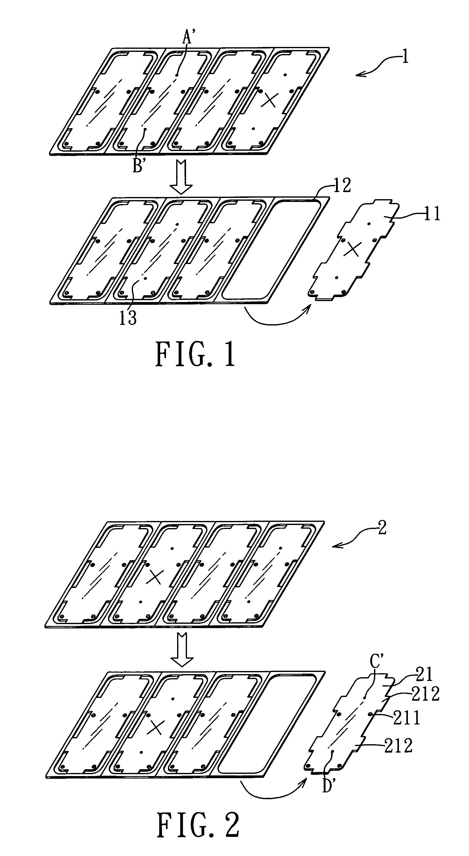
[0048] The board placement method and system for a defective printed circuit board panel having multiple interconnected PCB units according to the present invention is to use a good PCB unit of a defective printed circuit board panel having multiple interconnected PCB units for replacement in another defective printed circuit board panel so as to form a good repaired printed circuit board pair having multiple interconnected PCB units. Accordingly, referring to FIGS. 1 and 2, when there is a defective printed circuit board panel 1 having multiple interconnected PCB units, a defective PCB unit 11 is cut out and removed from the defective printed circuit board panel 1. A good PCB unit 21 is cut out from another defective printed circuit board panel 2 having multiple interconnected PCB units in the same manner for...


PUM

PropertyMeasurementUnit
currentaaaaaaaaaa
heightaaaaaaaaaa
height toleranceaaaaaaaaaa

Abstract

In a board placement method and system, a PCB panel having multiple interconnected PCB units and a vacant space is placed on a work surface of a reference platform. The work surface has an opening corresponding to the vacant space. The reference platform has a micro-adjusting unit, which includes a support seat disposed in the opening and movable along three directions. The support seat is used for placement of a good PCB unit. The current positions of the PCB panel and the good PCB unit are measured so as to calculate a target position of the good PCB unit and an error between the target position and the current position of the good PCB unit. The micro-adjusting unit can drive the support seat to move so as to move the good PCB unit to the target position. The good PCB unit is then fixed in the vacant space.

Description

CROSS-REFERENCE TO RELATED APPLICATION [0001] This application claims priority of Taiwanese Application No. 094136297, filed on Oct. 18, 2005. BACKGROUND OF THE INVENTION [0002] 1. Field of the Invention [0003] The invention relates to a board placement method and system for a defective printed circuit board panel having multiple interconnected printed circuit board units, more particularly to an automated board placement method and system for a defective printed circuit board panel having multiple interconnected printed circuit board units. [0004] 2. Description of the Related Art [0005] In the manufacture of a conventional printed circuit board panel, a plurality of independent printed circuit board units (hereinafter referred to as PCB units) are arranged and mounted on a substrate to form a printed circuit board panel having multiple interconnected PCB units so as to facilitate large-volume and quick component insertion on a production line. The defective product rate for printe...

Claims


Application Information

Patent Timeline
Patent Type & Authority Applications(United States)
IPC IPC(8): H01R13/648
CPCH05K1/0269Y10T29/4979H05K3/0052H05K3/0097H05K3/225H05K2201/10424H05K2203/166Y10T29/53004Y10T29/49771Y10T29/53091Y10T29/4973Y10T29/49789Y10T29/49764Y10T29/53087H05K3/0008
Inventor KU, SHING-SAN
Owner KU SHING SAN
Why Eureka
Try Eureka